NEO Semiconductor Unveils 1T1C and 3T0C IGZO-Based 3D X-DRAM Technology
delivers up to 512Gb density and 450-second retention with ultra-low power consumption — built on 3D NAND-compatible processes and optimized for AI, in-memory computing, and next-gen DRAM and HBM applications
This is a Press Release edited by StorageNewsletter.com on May 8, 2025 at 2:00 pmNEO Semiconductor announced the latest advancement in its 3D X-DRAM technology family — the industry-first 1T1C- and 3T0C-based 3D X-DRAM cell, a transformative solution designed to deliver unprecedented density, power efficiency, and scalability for the most demanding data applications.
![]()
The company unveils a breakthrough 1T1C-type 3D X-DRAM cell – delivering up to 512 Gb density, 10ns fast RW speed, and over 450 seconds of data retention – optimized for high-performance HBM and AI applications
Built on a 3D NAND-like architecture and with proof-of-concept test chips expected in 2026, the new 1T1C and 3T0C designs combine the performance of DRAM with the manufacturability of NAND, enabling cost-effective, high-yield production with densities up to 512Gb — a 10x improvement over conventional DRAM.
“With the introduction of the 1T1C and 3T0C 3D X-DRAM, we are redefining what’s possible in memory technology,” said Andy Hsu, founder and CEO, NEO Semiconductor. “This innovation pushes past the scaling limitations of today’s DRAM and positions NEO as a frontrunner in next-generation memory.”
Key Features and Benefits:
- Unmatched Retention and Efficiency – Thanks to IGZO channel technology, 1T1C and 3T0C cell simulations demonstrate retention times of up to 450 seconds, reducing refresh power.
- Verified by Simulation – TCAD (Technology Computer-Aided Design) simulations confirm fast 10-nanosecond RW speeds and over 450-second retention time.
- Manufacturing-Friendly – Uses a modified 3D NAND process, with minimal changes, enabling full scalability and rapid integration into existing DRAM manufacturing lines.
- Ultra-High Bandwidth – Employs unique array architectures for hybrid bonding to significantly enhance memory bandwidth while reducing power consumption.
- High Performance for Advanced Workloads – Designed for AI, edge computing, and in-memory processing, with reliable high-speed access and reduced energy consumption.
Expanding the 3D X-DRAM Family
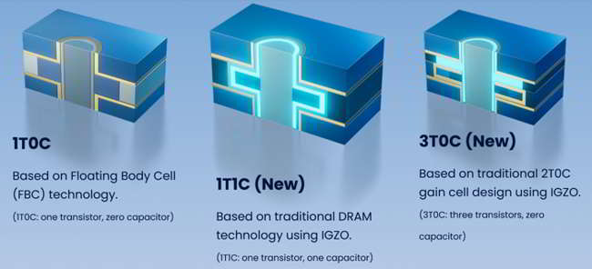
The company’s technology platform now includes three 3D X-DRAM variants:
-
1T1C (one transistor, one capacitor) – The core solution for high-density DRAM, fully compatible with mainstream DRAM and HBM roadmaps.
-
3T0C (three transistor, zero capacitor) – Optimized for current-sensing operations, ideal for AI and in-memory computing.
-
1T0C (one transistor, zero capacitor) – A floating-body cell structure suitable for high-density DRAM, in-memory computing, hybrid memory and logic architectures.
NEO’s IGZO-based 3D X-DRAM delivers up to 512Gb density and 450-second retention with ultra-low power consumption — built on 3D NAND-compatible processes and optimized for AI, in-memory computing, and next-gen DRAM and HBM applications; proof-of-concept test chips expected in 2026
NEO Semiconductor will attend the 17th IEEE International Memory Workshop, May 18th-21st 2025 in Monterey, CA, USA.


 Subscribe to our free daily newsletter


