SK hynix Multilayered 176-Layer 512Gb TLC 4D NAND Flash
Following Micron
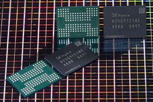
This is a Press Release edited by StorageNewsletter.com on December 18, 2020 at 2:15 pmSK hynix Inc. announced the completion of developing a multilayered 176-layer 512Gb TLC 4D NAND flash.
It provided the samples to controller companies last month to make a solution product.
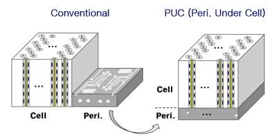
The firm has been promoting 4D technology from the 96-layer NAND flash products that combine Charge Trap flash (CTF) with high-integrated Peri. Under Cell (PUC) technology.
The 176-layer NAND flash is the third gen 4D product that secures the best number of chips per wafer. This allows the bit productivity to be improved by 35% compared to the previous gen with the differentiated cost competitiveness. The read speed of cell increased by 20% over the previous gen adopting 2-division cell array selection technology. The data transfer speed also has been improved by 33% to 1.6Gb/s adopting speed-up technology without increasing the number of processes.
Starting with mobile solution products that have improved maximum read speed by 70% and maximum write speed by 35% in the middle of next year, the company plans to release consumer and enterprise SSDs sequentially expanding its application market of the products.
As the number of layers increases in NAND flash, the cell current reduction, the channel hole twisting, and the cell distribution deterioration due to double stack misalignment occur. The company overcame these challenges by adopting technologies such as cell interlayer height reduction, layer variable timing control and precise alignment and developed the industry’s top tier-176-layer NAND flash.
The firm also plans to consistently enhance its competitiveness in the NAND flash business by developing 1Tb products with doubled density based on 176-layer 4D NAND.
“NAND flash industries are striving to improve technologies for high integration and maximum productivity at the same time,” said Jung Dal Choi, head, NAND development. “SK hynix, as a pioneer of 4D NAND, will lead the NAND flash market with the industry’s highest productivity and technology.”
According to market intelligence provider Omdia, the NAND flash market is estimated to expand from 431.8 billion GB in 2020 to 1.366 trillion GB in 2024 with 33.4% CAGR.
Annotation:
4D NAND
The company has named ‘4D NAND flash’ to highlight the differentiation that achieves both performance and productivity at the same time by combining CTF cell structure and PUC technology from 96-layer NAND flash in 2018.
Charge Trap Flash (CTF)

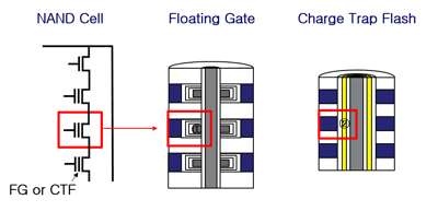
Unlike floating gate, which stores electric charges in conductors, CTF stores electric charges in insulators, which eliminates interference between cells, improving read and write performance while reducing cell area per unit compared to floating gate technology. Most 3D NAND companies are adopting CTF.
Peri. Under Cell (PUC)
 A technology that maximizes production efficiency by placing peripheral circuits under the cell array.
2-division cell array selection technology
The word line applies a voltage to the cell in the NAND flash circuit. The more the number of layers, the thinner the word line is to lower the cell’s height, and the greater the resistance applied to the word line will affect the speed. By dividing the cell connected to the word line into half compared to the existing one, the resistance can be lowered, which shortens the time of applying voltage and improves the read speed.
Cell interlayer height reduction technology
As the number of layers increases, it becomes difficult to drill holes for cell formation. This leads to increased resistance and reduced current, making it difficult to secure performance and reliability. For this, it is necessary to lower the cell interlayer height as much as possible, but this can increase interference between cells and defect rate. The cell interlayer height reduction technology lowered cell interlayer height of 176-layers and also secured competitive performance/reliability with related processes and design technologies.
Layer variable timing control technology
Increasing the number of layers and lowering the layer height often leads to channel hole twisting and cell scattering deterioration, which degrades the performance and reliability of each layer. This technology adjusts the amount and time of voltage applied according to the characteristics of each layers to maintain uniform cell characteristics and improve performance and reliability.
Ultra-precise alignment technology
Industries are utilizing a double-stack process that drills holes twice because it is impossible to drill holes for cell formation at once as the number of layers increases. Minimizing double-stack misalignment is the core of the double-stack technology. If the stacks are not aligned correctly, it will result in poor flow of current between stacks and occurrence of deterioration, reducing yield rate, performance and reliability. SK hynix applied double-stack technology since its 72-layer product in 2017, to this 176-layer product and a technology that automatically corrects the location and size of holes in real time based on its know-how.


 Subscribe to our free daily newsletter

