


Micron First to Ship Record 176-Layer NAND Flash Memory
SSDs will continue to be cheaper and more capacitive.
This is a Press Release edited by StorageNewsletter.com on November 18, 2020 at 2:16 pmMicron Technology, Inc. begun volume shipments of the first 176-layer 3D NAND flash memory, achieving industry-pioneering density and performance.
Together, the 176-layer technology and architecture represent a breakthrough, enabling gains in application performance across a range of storage use cases spanning data center, intelligent edge and mobile devices.
“Micron’s 176-layer NAND sets a new bar for the industry, with a layer count that is almost 40% higher than our nearest competitor’s,” said Scott DeBoer, EVP, technology and products. “Combined with Micron’s CMOS-under-array architecture, this technology sustains Micron’s industry cost leadership.“
Representing the company’s fifth gen of 3D NAND and second-gen replacement-gate architecture, the 176-layer NAND is a technologically advanced NAND node. Compared with the company’s previous gen of high-volume 3D NAND, the 176-layer NAND improves both read latency and write latency by more than 35% – accelerating application performance. (1) Featuring approximately 30% smaller die size than best-in-class competitive offerings, 176-layer NAND’s compact design is for solutions using small form factors.
Groundbreaking technology arms diverse markets with fullest power of flash
“Micron’s 176-layer NAND enables breakthrough product innovation for our customers,” said Sumit Sadana, EVP and chief business officer. “We are deploying this technology across our broad product portfolio to bring value everywhere NAND is used, targeting growth opportunities in 5G, AI, cloud and the intelligent edge.“
With its versatile design and density, the 176-layer NAND serves as a building block in technologists’ toolboxes across an array of sectors, including mobile storage, autonomous systems, in-vehicle infotainment, and client and data center SSDs.
It offers improved QoS (2), a critical design criterion for data center SSDs. (3) This can accelerate data-intensive environments and workloads such as data lakes, AI engines and big data analytics. For 5G smartphones, the enhanced QoS can enable faster launching and switching across multiple apps, creating a responsive mobile experience and enabling multitasking and full use of 5G’s low-latency network.
The company’s fifth gen of 3D NAND also features a maximum data transfer rate at 1,600 megatransfers per second (MT/s) on the Open NAND flash Interface (ONFI) bus, a 33% improvement. (4) The increased ONFI speed leads to faster system bootup and application performance. In automotive applications, this speed will power near instant-on response times for in-vehicle systems as soon as engines are turned on, enhancing the user experience.
The company is working with industry developers to integrate the new products into solutions. To simplify firmware development, the 176-layer NAND offers a single-pass programming algorithm, enabling integration and speeding time to market.
Achieves density and cost leadership with novel architecture
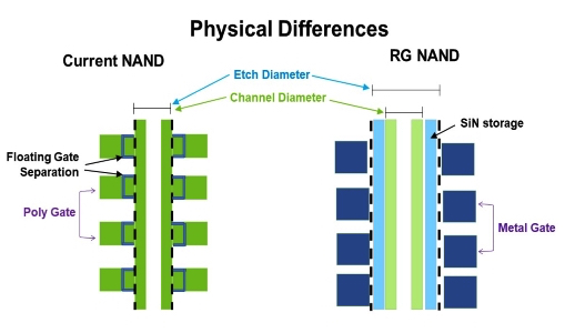
With the slowing of Moore’s Law, Micron’s innovation in 3D NAND is critical to ensuring that the industry can keep pace with growing data requirements. To achieve this milestone, the company has combined its stacked replacement-gate architecture, novel charge-trap and CMOS-under-array (CuA) (5) techniques. The company’s 3D NAND experts achieved rapid advancements with the firm’s proprietary CuA technique, which constructs the multilayered stack over chip’s logic – packing more memory into a tighter space and substantially shrinking the 176-layer NAND’s die size, yielding more gigabytes per wafer.
In tandem, the company has improved scalability and performance for future NAND gens by transitioning its NAND cell technology from legacy floating gate to charge-trap. This charge-trap technology is combined with the company’s replacement-gate architecture, which uses highly conductive metal wordlines (6) instead of a silicon layer to achieve 3D NAND performance. The firm’s adoption of this technology will also enable the company to drive cost reductions.
Applying these techniques, Micron has increased endurance, which is particularly beneficial in write-intensive use cases – from black boxes in aerospace to video surveillance recording. In mobile storage, 176-layer NAND’s replacement-gate architecture results in 15% faster mixed workload performance (7) to power fast edge computing, enhanced AI inference, and graphic-rich, real-time multiplayer gaming.
Availability:
The company’s 176-layer triple-level cell 3D NAND is in volume production in the firm’s Singapore fab and shipping to customers, including through its Crucial consumer SSD product lines. The company will introduce additional new products based on this technology during calendar 2021.
(1) Comparison is based on Micron’s high-volume, floating-gate 96-layer NAND. When comparing with 128-layer replacement-gate NAND, read latency and write latency for Micron’s 176-layer NAND both improve by over 25%.
(2) QoS refers to the consistency and predictability of SSD response times.
(3) Improved QoS is driven by a reduction in block size and less variance in read latency, as compared to Micron’s high-volume, floating-gate 96-layer NAND.
(4) Improvement is over Micron’s prior two gens of 3D NAND (96-layer NAND and 128-layer NAND) which featured a maximum of 1,200MT/s data transfer rates.
(5) CMOS stands for complementary metal oxide semiconductor.
(6) Wordlines are connecting wires to the gate of each NAND memory storage element in a NAND memory array. They are used to select, program and erase groups of memory cells in an array of NAND memory.
(7) This is compared to Micron’s previous gen universal flash storage 3.1-based multichip package using floating-gate 96-layer NAND.
Resources:
Product page: 176-layer NAND
Blog: Doing What Can’t Be Done (Again) — Micron Ships 176-Layer NAND
Micron Transitions to Next-Gen 3D NAND Replacement-Gate Technology
Video: Taking 176-Layer Flash Memory from Lab to Fab
Video: Just How Remarkable Is Micron’s 176-Layer 3D Flash Memory?
Read also:
Micron 2300 and 2210 QLC M.2 Up to 2TB NVMe Client SSD With 96-Layer 3D NAND
Up to 3,300MB/s and 2,700MB/s sequential RW speeds for 2300, 2,200MB/s and 1,800MB/s sequential RW speeds for 2210 QLC
May 19, 2020 | Press Release
Micron Open-Source Heterogeneous-Memory Storage Engine Designed for SSDs and Storage-Class Memory
Optimizes throughput, latency and endurance, available to open-source community for developers using all-flash infrastructure who require benefits of open-source software.
May 7, 2020 | Press Release
Micron: 5210 ION Enterprise SATA 2.5-Inch Up to 7.7TB SSD With QLC NAND
Up to 540MB/s and 360MB/s sequential RW speeds, 90,000/4.500 IO/s random RW for 7.7TB model
April 13, 2020 | Press Release
Comments
SSDs will continue to be cheaper and more capacitive.
It's proved by this Microns's announcement of 176-layer triple-level cell 3D NAND flash memory, even already produced in volume in its Singapore's fab, according to the company.
Click to enlarge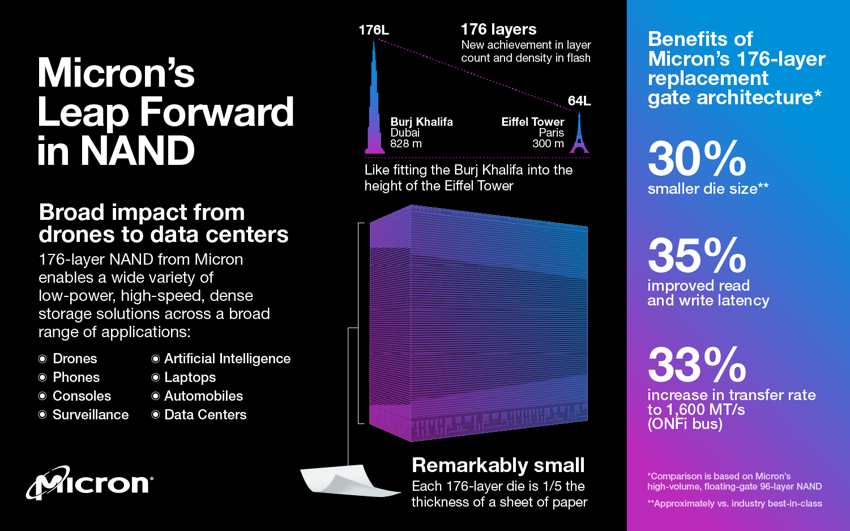
First products integrating this technology will be Micron's Crucial consumer SSDs, then other ones especially enterprise SSDs next year.
It will probably replaced previous company's generation with 96 and 128 layers. The new technology is the Micron's fifth gen of 3D NAND and second-gen replacement-gate architecture.
But an analyst said that adding layers could affect the reliability.
The new technology reaches 1,600MT/s with reads improved by over 35% and writes by 25% compared to former generation.
The first parts are Micron's 512Gb TLC dies, built using string stacking of two 88-layer decks.
Company's CMOS-under-array (CuA), charge-trap, and replacement-gate architectures have been used in tandem to squeeze together 176 layers of ultra-dense memory.
Replacement-Gate Technology
By reducing cell-to-cell capacitive coupling issues and mitigating resistance with a metal control gate, Micron's replacement-gate (RG) NAND is part of a high-capacity data storage system providing superior performance.
176-layer die can hold 20-30 hours of 1,920x1,080p video.
Other manufacturers are involved in 176 layers, but Micron is first to start volume shipments with NAND leader Samsung hoping to produce V-NAND flashes with 170 or more layers during 1H21 and SH hynix 176-layer 4D NAND flash at about the same time. Intel announced 144 layers last May. Yangtze Memory Technologies Co. from China is also intending to mass produce 128-layer NAND by the end of 2020.


 Subscribe to our free daily newsletter


