



Sandisk Announces Sampling of BiCS10 1Tb TLC 3D NAND Flash Memory Pushing Density, Power Efficiency and Performance to Support Data-Intensive Workloads
BiCS10 TLC delivers up to 4.8Gb/s NAND interface speed, 59 percent bit density improvement compared to BiCS8 and enhanced power efficiency
This is a Press Release edited by StorageNewsletter.com on July 8, 2026 at 2:01 pmSandisk Corp. announced it is sampling its BiCS10 1Tb TLC, its 10th-generation 3D NAND flash memory technology. BiCS10 applies advanced lateral scaling techniques to achieve industry-leading 1Tb TLC memory density greater than 29Gb/mm, improving bit density by 59% while delivering up to 4.8Gb/s interface speed, a 33% improvement compared with 8th generation 3D flash memory currently in mass production.
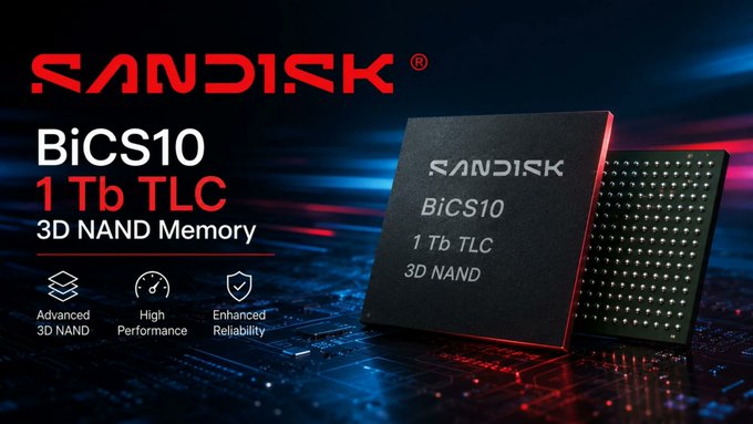
Built on Sandisk’s proven Bit-Cost Scalable (BiCS) 3D NAND architecture and CMOS directly Bonded to Array (CBA) technology, BiCS10 TLC also enhances data input/output power efficiency, reducing power consumption by 10% for input and 34%for output compared to the previous BiCS8 generation.
“As the world becomes more connected, data-intensive and intelligent, NAND plays an increasingly mission-critical role in delivering the performance, efficiency and scale modern computing requires,” said Alper Ilkbahar, CTO, Sandisk. “BiCS8 set a new benchmark for 3D NAND by combining our wafer bonding capabilities with meaningful gains in density, performance, and efficiency. With BiCS10 TLC, we build upon that proven foundation to deliver faster interface speeds, higher bit density and improved power efficiency for our customers.”
NAND flash memory is one of the most scalable semiconductor technologies today, and the foundation of what Sandisk builds. BiCS10 advances Sandisk’s long-term roadmap for scaling NAND through continued innovation in density, power efficiency, and architecture. It builds upon Sandisk’s CBA technology, which fabricates CMOS logic and the memory array on separate wafers before bonding them together with high-precision wafer-to-wafer alignment. BiCS10 TLC increases the number of memory layers to 332 and incorporates Toggle DDR6.0, SCA protocol and PI-LTT technology to support high-speed, low-power operation.
The sampling milestone extends Sandisk’s BiCS roadmap with advancements that push density, power efficiency, and endurance in ways designed to support the next generation of data-intensive and AI-driven workloads. Key BiCS10 TLC technology highlights include:
- Up to 4.8Gb/s NAND interface speed, a 33% improvement
- 332 memory layers with optimized floor plan efficiency, improving bit density by 59%
- Enhanced data input/output power efficiency, reducing power consumption by 10% for input and 34% for output
- Support for Toggle DDR6.0, SCA protocol and PI-LTT technology to enable high-speed, low-power operation
Sandisk leads the way in flash innovation, from increasing bits per cell over time to advancing technologies in controller architecture, firmware, packaging, and system flash that improve the performance, efficiency, and utility of flash at scale. With a unique portfolio of leading IP and global manufacturing footprint, Sandisk controls its entire production lifecycle from design to manufacturing to final assembly with global operations, resulting in exceptional quality control, cost efficiency, faster time to market, and strong supply chain resilience.
Comments
This announcement was expected and as the annual rendez-vous, the FMS conference is coming in a few weeks, we see news...but above all it is a natural step.
The chip is built jointly with long-time manufacturing partner Kioxia under their BiCS architecture, and represents the latest step in a roadmap that has defined the two companies' NAND collaboration for over a decade.
Specifications are interesting with 332 memory layers, an areal bit density exceeding 29Gb/mm², which the company calls industry-leading, and a 59% improvement in bit density versus BiCS8. Interface speed reaches up to 4.8Gb/s using Toggle DDR6.0, a 33% improvement over the prior generation, alongside SCA protocol and PI-LTT technology, both aimed at cutting data input/output latency and power draw. Power efficiency gains are notable: a 10% reduction in input power consumption and a 34% reduction on the output side compared with BiCS8.
Architecturally, BiCS10 continues to rely on Sandisk's CBA technology, which fabricates the logic/peripheral circuitry and the memory cell array on two separate wafers before precision-bonding them together, the same wafer-bonding approach that differentiated BiCS8.
Sandisk is only sampling BiCS10 at this stage; volume production timing and initial SSD/product integration were not disclosed, and, as with any press release, forward-looking claims around performance and market positioning carry the usual execution risk (yield ramp, qualification cycles, and customer adoption timelines).
With exacale rack in mind and clear goal for the industry, BiCS10's 1Tb TLC die is aimed squarely at the enterprise SSD and hyperscale storage segment, where bit density directly drives drive capacity (multi-terabyte and eventually multi-hundred-terabyte SSDs) and cost-per-bit, the metric that ultimately governs data center storage economics. Layer count and lateral scaling (rather than simply adding more layers) have become the two competing paths to density gains as NAND makers approach practical limits on vertical stacking; Sandisk's emphasis on "lateral scaling techniques" for BiCS10 signals it is leaning on cell-shrink and array efficiency rather than layer count alone (332 layers is a meaningful but not industry-leading jump versus rivals' announced roadmaps).
Competition is obviously very active:
- Kioxia, Sandisk's manufacturing partner and joint IP holder for BiCS, is simultaneously a fierce commercial rival in SSDs. Kioxia's market value topped ¥10 trillion in January 2026, just over a year after its December 2024 IPO, driven by soaring NAND prices, and the company is also targeting SSDs nearly 100 times faster than current models, developed with NVIDIA for generative AI servers that could connect directly to GPUs and partially replace HBM. Kioxia has also publicly declared an intent to reclaim the industry's number-one NAND position
- SK hynix with its Solidigm subsidiary, plans to begin shipping 321-layer QLC NAND products in the second half of 2026, targeting a significant expansion of market share, pushing higher-density QLC as the preferred format for AI/enterprise capacity needs
- Samsung, the long-standing NAND share leader, accelerating investment in QLC NAND with its 286-layer V9 product as flagship, ramping Pyeongtaek Plant 4 and select Xi'an lines, with enterprise customers prioritized in the ramp
- Micron, competing on both layer-count roadmaps and geographic capacity expansion, including large Japan and Singapore investments as it works to close the gap with the top two Korean players while also redirecting wafer capacity toward HBM
- Phison is not a NAND fab owner but worth mentioning here as it is the dominant independent controller/IP supplier, holding long-term strategic partnerships with Kioxia, Micron, Sandisk, Samsung, SK hynix and YMTC, with more than 80% of revenue coming from "high-value" NAND storage markets such as servers, automotive and generative AI. Its enterprise Pascari line has pushed into ultra-high-capacity territory, with the D206V delivering up to 245.76TB in a single U.2 PCIe Gen5 SSD, illustrating how controller-side innovation is now as important to capacity scaling as the underlying NAND die itself
In terms of market share, positions are well established and even considered as solid with Samsung holding roughly 29% and SK hynix 18% of global NAND in Q1 2026, with Kioxia (14%), Micron (13%), Sandisk (13%) and YMTC (13%) all within a five-point range of each other, meaning any capacity or technology misstep can quickly reshuffle rankings.
BiCS10's launch lands squarely inside the most severe NAND shortage in over a decade. NAND flash contract prices are projected to rise 70–75% quarter-over-quarter in Q2 2026, outpacing DRAM for the first time in the current cycle, driven by enterprise SSD demand tied to generative AI deployments. Samsung, Micron and SK hynix jointly control roughly 63% of NAND supply, with production discipline, not a classic cyclical shortfall, driving allocation exhaustion, since new fab capacity isn't expected to reach meaningful volume before late 2027 or 2028.
FMS will be very interested.







 Subscribe to our free daily newsletter