IEEE Roadmap Outlines Development of Mass Digital Storage Technology
Report outlines current technology and expected advances and applications in digital storage and NVM technology for future.
This is a Press Release edited by StorageNewsletter.com on October 2, 2024 at 2:01 pmComputer has published on August 30, 2024 an article written by Tom Coughlin, Coughlin Associates, Inc., San Jose, CA, USA, and Roger Hoyt, consultant, San Jose, CA, USA.
Abstract: “The new IEEE International Roadmap for Devices and Systems Mass Data Storage report outlines the current technology and expected advances and applications in digital storage and nonvolatile memory technology for the future.“
Digital storage and nonvolatile memories enable advanced computing architectures as well as popular consumer and industrial applications. Steady advances in these technologies have provided a hierarchy of devices that allow system designers to find the optimal tradeoff of cost versus performance, particularly for large storage applications, such as data centers.
In 2024 the IEEE International Roadmap for Devices and Systems (IRDS) released a technical roadmap report on Mass Data Storage. We were the co-chairs of the committee that produced this report. The committee included experts on various storage and nonvolatile memory technologies. The report is available as a free download from IEEE. This activity is the continuation of a bi-annual Mass Storage Roadmap effort that we led with iNEMI for many years.
Other participants in the Mass Storage Roadmap team who contributed to the latest report include Ed Childers (IBM), Ron Dennison, Simeon Furrer (IBM), John Hoffman (Ernst & Young), Dave Landsman (Western Digital), Mark Lantz (IBM), Kevin Lu (Folio Photonics), Niranjan Natekar (Western Digital), Ken Singer (Folio Photonics), and Doug Wong (Kioxia).
In addition to the direct committee participants, the team included input from other IRDS road maps, particularly regarding solid-state storage and nonvolatile memories. Other material referenced included information from the INSIC tape storage roadmap, the Advanced Storage Research Consortium HDD roadmap, HDD road maps from Seagate, Western Digital, and Toshiba, and the LTO storage roadmap.
The report covers HDDs, magnetic tape, and optical disk technology as well as solid-state storage. In addition, there is material in the report correlated with other IRDS road maps on nonvolatile memory technologies, such as magnetic MRAM, resistive RAM (ReRAM), ferroelectric RAM (FeRAM), and phase-change memory (PCM). There is also a section on the use of DNA for archive storage.
Solid-State Storage and Nonvolatile Memory
Solid-state storage is dominated by NAND flash, currently a $60 billion market. NAND flash is the mass storage in most SSDs. Alternative nonvolatile memory technologies, such as MRAM, FeRAM, ReRAM, and PCM, are still more costly per bit but are being used in embedded devices for consumer and industrial applications to replace NOR flash and some static RAM (SRAM) (especially MRAM and ReRAM). 2024 is a recovery year for all storage and memory technologies after 2022 and 2023, which were down years because of the time it took to consume excessive inventories acquired during supply uncertainties during the Covid pandemic.
Future developments for higher capacity NAND flash include higher layer counts and more bits per cell. However, the cost reductions from adding more layers are becoming less noticeable, and more bits per cell come with lower endurance and performance.
Future developments for higher capacity NAND flash include higher layer counts and more bits per cell.
Table 1. NAND flash chip road map

For 3D stacked NAND flash cells, the memory transistor is a larger cylindrically shaped cell that can store more charge than the prior generation and shrinking 2D cell and has made possible the transition from 2 bits per cell to 3 bits per cell. For some applications, QLC is also now available. Demonstrations of 5 bits per cell [penta-level cells (PLCs)] have also been done.
Current NAND flash products stack hundreds of layers in tiers to achieve a higher areal density per die. For each additional layer in the 3D NAND, there is an incremental increase in die density but also an incremental increase in wafer processing time and thus in the cost per wafer. As a consequence, the decrease in cost per bit does not directly follow the increasing die density as the number of layers increases.
The decrease in cost per bit does not directly follow the increasing die density as the number of layers increases.
The path to continuing increasing the die density and reducing the cost per bit will involve minimizing the growth in layer count, increasing the density of memory cells per layer (increasing the areal density per layer), decreasing the size of the holes where the memory cells are manufactured, increasing the number of bits stored per transistor TLC to QLC to PLC, and maintaining a uniform high aspect ratio etch for each memory hole. These are design and manufacturing issues and must be solved to maintain the high production yields necessary for profitable manufacturing.
Ultimately, there will be a limit to the number of layers that 3D NAND can practically achieve, but it will be some time before that limit is reached. As of 2024, projections of up to 1,000 layers have been discussed.
Embedded NOR flash, used for code storage in embedded devices, has reached a scaling limit at 28 nm, and this has opened up opportunities to replace embedded NOR with persistent memories that can scale to a smaller size. MRAM and ReRAM are beginning to replace NOR flash in some embedded products. Likewise, embedded SRAM may also face scaling limits at around 14 nm, and SRAM cells are very large because of the many transistors they use. For this reason, there are some embedded devices that are starting to use MRAM or ReRAM to replace slower SRAM caches, particularly to support AI inference applications.
HDDs
The total unit shipment of HDDs continues to decline, with legacy HDD applications being replaced by SSDs. However, the data center and enterprise nearline HDD market has recovered in 2024, and demand continues to grow for HDD storage in big data applications, including AI, driven by the lower cost per bit for HDD storage.
Demand continues to grow for HDD storage in big data applications, including AI, driven by the lower cost per bit for HDD storage.
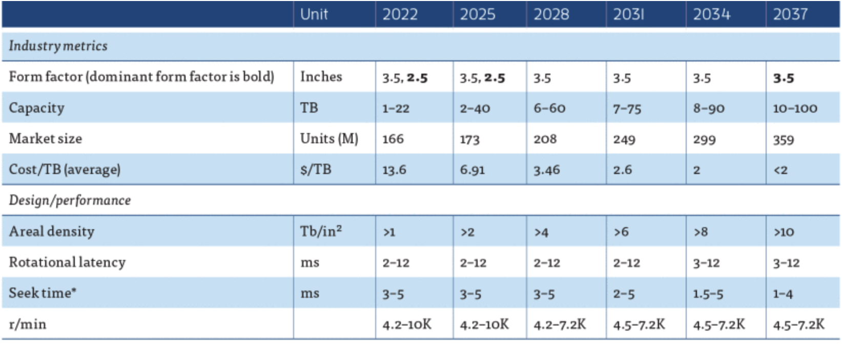
These high-capacity drives are sealed and filled with helium, have up to 10 disks, and may include dual actuators, HAMR, and 2D magnetic recording (TDMR). Current storage capacities are up to 32TB, but 50TB HDDs should be available by 2026–2027. This should allow HDDs to continue to be competitive against SSDs for secondary storage and active archive applications.
Table 2. Magnetic Mass Data Storage Technology Roadmap: HDD

Critical advances are required in magnetic and nonmagnetic materials for functional HDD head read and write performance at high areal densities and operating at high data rates. These advances include improvements in disk media and overcoats as well as heads capable of supporting densities in excess of 160Gb/cm2 (1,000 Gb/in2 or 1 Tb/in2), changes in media substrate technology, and dielectric films less than 1nm thick for advanced GMR and tunneling magnetoresistive (TMR) heads.
In addition, technologies such as shingled magnetic recording, TDMR, HAMR, (an example of energy-assisted magnetic recording (EAMR)(, and heated-dot magnetic recording will require HDD designs with new processes and materials.
Seagate Technology began shipping 30+TB HAMR HDDs for data center evaluation and qualification starting in 2022 and is shipping these products in volume in 2H24. Toshiba also announced that it will ship 30+TB HAMR and microwave-assisted magnetic recording HDDs by 2025. By 2026–2027, 50+TB HDDs will be possible using EAMR.
Magnetic TapeLinear tape technology uses the same basic magnetic recording principles as HDDs and leverages many of the technologies developed by the higher volume and more advanced HDD industry. Magnetic tape is often used in library systems, which combine robotics, tape cartridges, and tape drives to provide low-energy archival mass storage of data.
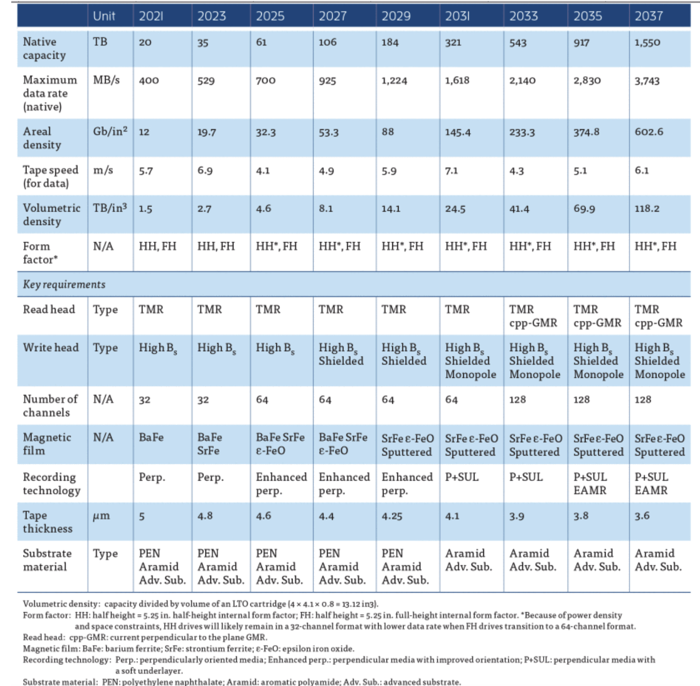
Magnetic half-inch tape native capacities are currently available up to 50TB (the latest generation IBM enterprise tape). Magnetic tape cartridges don’t consume a lot of energy except when they are in a drive. Tape is also significantly less expensive per byte of stored data than HDDs. Thus, tape provides a low-cost and compact archival storage. Cartridges with greater than 100TB native capacity should be available in future generations.
The current tape market is dominated by the LTO format with a smaller share held by the IBM TS11xx enterprise format. Current LTO media manufacturers include Sony as well as Fujifilm, who also manufactures media for IBM’s TS11xx tape drives. HPE, IBM, and Quantum all provide technology provider company-certified LTO drives. Multiple companies, including Dell, Fujitsu, HPE, IBM, Quantum, Spectra Logic, Tandberg, etc., offer tape library solutions.
Table 3. Magnetic Mass Data Storage Technology Roadmap: Tape

Tape media recording performance improvements are typically achieved through a combination of technologies that include reducing the size of the magnetic particles in the recording layer to reduce media noise, developing new magnetic particles with improved magnetic properties, improving the dispersion of the magnetic particles, orienting the particles during the coating process, reducing variations in the thickness of the recording layer, and reducing the media roughness to improve the magnetic spacing.
Linear tape cartridges have sustained about a 30%-40% annual growth rate in storage capacity over the last decade through the combination of breakthroughs in four areas. These are the incorporation of MR, GMR, and TMR heads for reading data from the tape, advances in track-following servo technology, advances in error correction codes and data channels, and also advances in media technology (described previously).
To achieve the areal densities projected in the later phases of the magnetic tape road map will require the development of ultrathin wear coatings and very smooth media so that the head–tape spacing can approach that used in current HDD products. In addition, the development of low-friction head technologies that optimize the geometry and topography of the tape-bearing surface will be required to enable the use of such very smooth media. An alternative strategy to address the spacing challenge is to move away from the current use of contact recording and adapt a form of the air-bearing technology developed for HDDs for use in tape recording.
Increasing the track density in linear tape recording will require improvements to the track-following servo systems. These will include improvements in the process that originally records the servo information on the tape and improvements in the servo system’s ability to follow the tracks on a flexible media during reading and writing.
Optical Disks
Optical disk technology has declined as a consumer media distribution media, and the focus on new optical storage products is on their use as a low-cost archival storage medium.
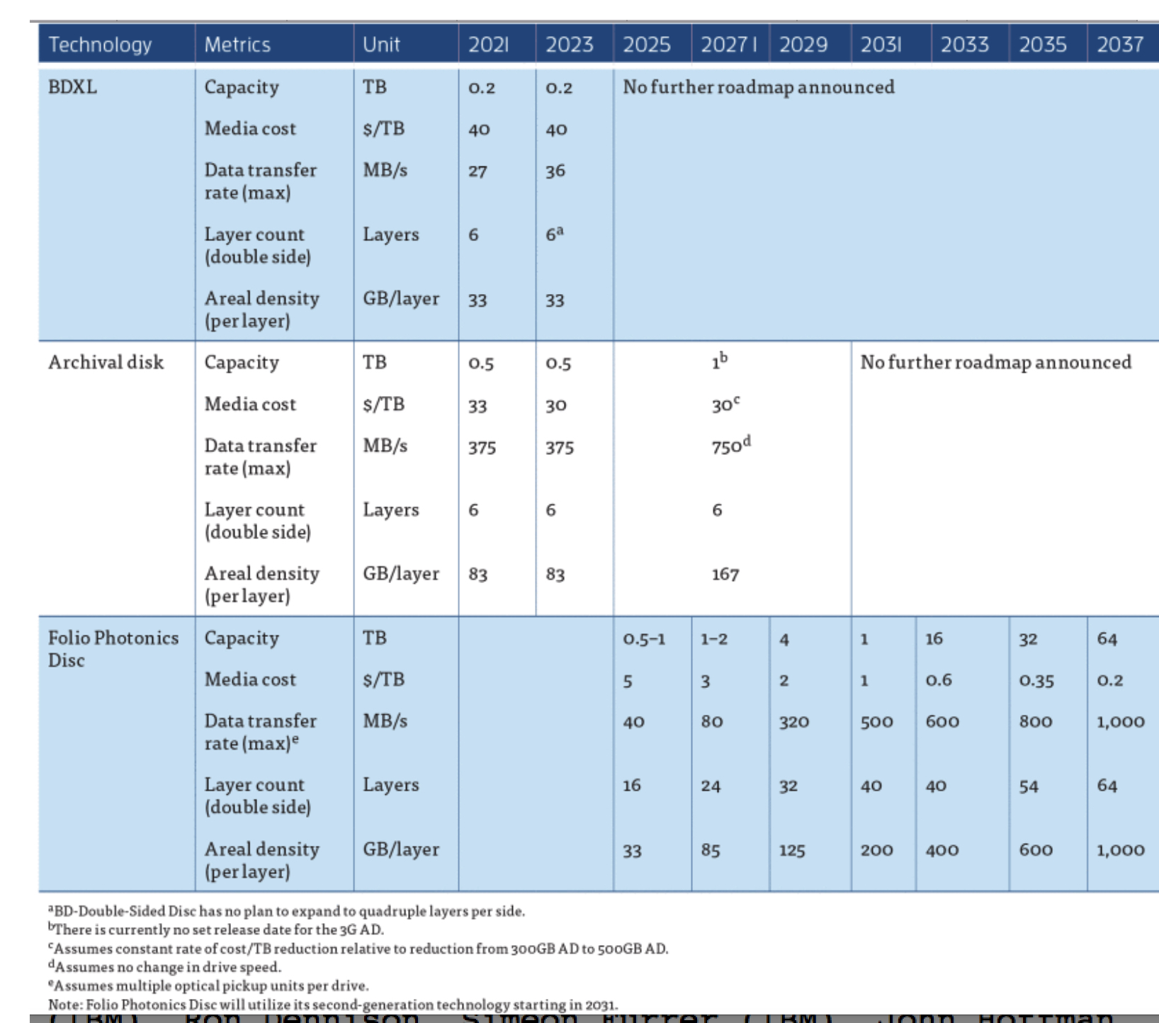
Write-once 100TB optical disks are projected in the near future, and this optical storage will likely be housed in optical library systems. Optical libraries face competition from magnetic tape libraries, which are more established for archival storage applications.
Table 4. Optical Mass Data Storage Technology Roadmap

Optical storage media and recording with modern materials can physically last more than 100 years. This makes this media interesting for long-term archiving applications. Optical disks also consume little energy when not in use in a library system, similar to tape cartridges in a tape library. However, technology obsolescence may make it more economical and necessary to migrate data from an older archive medium to new media, even if the existing medium is sound, so that data remain accessible.
The major challenges to optical storage library systems are creating high media capacity at a low cost and with fast enough read and write speeds. There are several efforts WW to develop next-gen archival optical storage solutions for data center library applications.
DNA Storage
DNA storage has been demonstrated in the lab, but the costs of reading and writing data on synthetic DNA are currently too expensive for practical applications. However, because of the rate of technological development of genomics for medical applications, the costs of reading and writing synthetic DNA are dropping, and this could make DNA an affordable alternative for archive storage in the near future. DNA storage will probably be in some sort of library system like magnetic tape or optical disks. Much work is needed to create a manufacturable and cost-effective DNA storage system.
DNA storage has been demonstrated in the lab, but the costs of reading and writing data on synthetic DNA are currently too expensive for practical applications.
Initially at least, synthetic DNA storage will complement rather than replace other digital storage media. The first use cases of synthetic DNA will likely be for deep/cold archives (100+ years duration), with Write Once/Read Never-to-Seldom access patterns, and assuming no additions or changes to the data during storage. For customers with such use cases, the value of the data may outweigh the high (relative to incumbent media) cost of writing and reading as well as (again relative to incumbent media) low throughput and high latency (time to first byte).
Digital storage demand is increasing, and this creates a need for more advanced storage technologies to support a robust digital mass storage hierarchy. The IEEE IRDS Mass Storage Roadmap provides projections for NAND flash, emerging nonvolatile memories, HDDs, magnetic tape, optical recording, and DNA storage development.
These different storage technologies exist in a hierarchy, and larger storage facilities will likely use multiple types of digital storage together to find an optimal balance between performance and cost of storage.


 Subscribe to our free daily newsletter


