









Pohang University of Science and Technology Researchers in Korea Announces Breakthrough in Next-Gen Memory Technology
Significantly enhanced storage capacity of ferroelectric memory devices
This is a Press Release edited by StorageNewsletter.com on June 19, 2024 at 2:01 pmFrom Pohang University of Science and Technology (POSTECH)
A research team led by Professor Jang-Sik Lee, department of materials science and engineering and department of semiconductor engineering, Pohang University of Science and Technology (POSTECH), has significantly enhanced the storage capacity of ferroelectric (1) memory devices.
Fig. 1. Structure and design strategy of MFMFS-FeTFT.
(A) Schematic of MFMFS-FeTFT with an AMFS/AMFM ratio of 1. AMFS, AMFM, dMFS, and dMFM represent the area of capacitors and thickness of the ferroelectric layers in the MFS and MFM regions. (B) Relationship between memory window and the capacitance ratio of MFMFS-FeTFTs with an AMFS/AMFM ratio of 1 and 5. (C) Transfer characteristics of the MFMFS-structured FeTFT with an area ratio of 1 and dMFS of 2 nm.
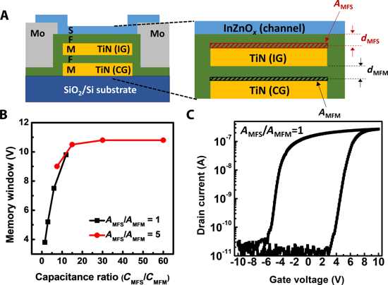
By utilizing hafnia-based ferroelectric materials and an innovative device structure, their findings, published on June 7 in the international journal Science Advances, mark a substantial advancement in memory technology.
With the exponential growth in data production and processing due to advancements in electronics and AI, the importance of data storage technologies has surged. NAND flash memory (2) , one of the most prevalent technologies for mass storage, can store more data in the same area by stacking cells in a 3D structure rather than a planar one. However, this approach relies on charge traps to store data, which results in higher operating voltages and slower speeds.
Recently, hafnia-based ferroelectric memory has emerged as a promising next-gen memory technology. Hafnia (Hafnium oxide) enables ferroelectric memories to operate at low voltages and high speeds. However, a significant challenge has been the limited memory window for multilevel data storage.
Professor Jang-Sik Lee, team, POSTECH, has addressed this issue by introducing new materials and a novel device structure. It enhanced the performance of hafnia-based memory devices by doping the ferroelectric materials with aluminum, creating high-performance ferroelectric thin films. Additionally, it replaced the conventional metal-ferroelectric-semiconductor (MFS) structure, where the metal and ferroelectric materials that make up the device are simply arranged, with an innovative metal-ferroelectric-metal-ferroelectric-semiconductor (MFMFS) structure.
The team successfully controlled the voltage across each layer by adjusting the capacitance of the ferroelectric layers, which involved fine-tuning factors such as the thickness and area ratio of the metal-to-metal and metal-to-channel ferroelectric layers. This efficient use of applied voltage to switch ferroelectric material improved the device’s performance and reduced energy consumption.
Conventional hafnia-based ferroelectric devices typically have a memory window of around 2V. In contrast, the research team’s device achieved a memory window exceeding 10V, enabling QLC (3) technology, which stores 16 levels of data (4 bits) per unit transistor. It also demonstrated high stability after more than one million cycles and operated at voltages of 10V or less, significantly lower than the 18V required for NAND flash memory. Furthermore, the team’s memory device exhibited stable characteristics in terms of data retention.
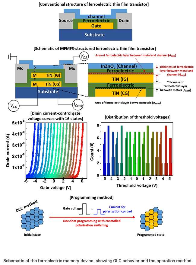
NAND flash memory programs its memory states using Incremental Step Pulse Programming (ISPP), which leads to long programming times and complex circuitry. In contrast, the team’s device achieves rapid programming through one-shot programming by controlling ferroelectric polarization switching.
Professor Jang-Sik Lee, POSTECH, commented, “We have laid the technological foundation for overcoming the limitations of existing memory devices and provided a new research direction for hafnia-based ferroelectric memory.”
He added: “Through follow-up research, we aim to develop low-power, high-speed, and high-density memory devices, contributing to solving power issues in data centers and AI applications.”
The research was conducted with the support from the Project for Next-generation Intelligent Semiconductor Technology Development of the Ministry of Science and ICT (National Research Foundation of Korea) and Samsung Electronics.
(1) Ferroelectrics : Materials with spontaneous electric polarization that can be reversed by an external electric field, used for non-volatile memory.
(2) NAND flash memory : A type of non-volatile storage that uses charge-trap transistors to trap electrical charges, offering high storage density.
(3) QLC operation : A NAND flash technology that stores 4 bits per cell by distinguishing 16 data levels, increasing storage density.
Article: Unlocking large memory windows and 16-level data per cell memory operations in hafnia-based ferroelectric transistors
Science Advances has published an article written by Ik-Jyae Kim, and Jang-Sik Lee, Department of Materials Science and Engineering, POSTECH, Pohang 37673, Korea.
Abstract: “Ferroelectric transistors based on hafnia-based ferroelectrics exhibit tremendous potential as next-generation memories owing to their high-speed operation and low power consumption. Nevertheless, these transistors face limitations in terms of memory window, which directly affects their ability to support multilevel characteristics in memory devices. Furthermore, the absence of an efficient operational technique capable of achieving multilevel characteristics has hindered their development. To address these challenges, we present a gate stack engineering method and an efficient operational approach for ferroelectric transistors to achieve 16-level data per cell operation. By using the suggested engineering method, we demonstrate the attainment of a substantial memory window of 10V without increasing the device area. Additionally, we propose a displacement current control method, facilitating one-shot programming to the desired state. Remarkably, we suggest the compatibility of these proposed methods with 3D structures. This study underscores the potential of ferroelectric transistors for next-generation 3D memory applications.“








 Subscribe to our free daily newsletter


