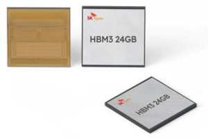
SK hynix Provides Samples of First 12-Layer HBM3 24GB Memory
Can process up to 819GB/s, meaning that 163 FHD movies can be transmitted in single second.
This is a Press Release edited by StorageNewsletter.com on April 27, 2023 at 2:01 pm- Develops HBM3 product with industry’s largest 24GB memory capacity; customers’ performance evaluation of samples underway
- Features high-capacity and high-performance through stacking of 12 DRAM chips
- Plans to complete preparation for mass production by 1H23, aimed at solidifying company’s leadership in DRAM market
SK hynix Inc. has become an industry’s 1st to develop 12-layer HBM3 (1) product with a 24GB (2) memory capacity, currently the largest in the industry, and said customers’ performance evaluation of samples is underway.
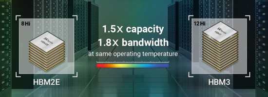
“The company succeeded in developing the 24GB package product that increased the memory capacity by 50% from the previous product, following the mass production of the world’s first HBM3 in June last year,” the company said. “We will be able to supply the new products to the market from the second half of the year, in line with growing demand for premium memory products driven by the AI-powered chatbot industry.”
The firm’s engineers improved process efficiency and performance stability by applying Advanced Mass Reflow Molded Underfill (MR-MUF) (3) technology to the latest product, while Through Silicon Via (TSV) (4) technology reduced the thickness of a single DRAM chip by 40%, achieving the same stack 8 level as the 16GB product.
The HBM, first developed by the company in 2013, has drawn broad attention from the memory chip industry for its role in implementing generative AI that operates in HPC systems.
The latest HBM3 standard, in particular, is considered the optimal product for rapid processing of large volumes of data, and therefore its adoption by major global tech companies is on the rise.
The firm has provided samples of its 24GB HBM3 product to multiple customers that have expressed expectation for the latest product, while the performance evaluation of the product is in progress.
Click to enlarge
“SK hynix was able to continuously develop a series of ultra-high speed and high capacity HBM products through its leading technologies used in the back-end process,” said Sang Hoo Hong, head, package and test, SK hynix. “The company plans to complete mass production preparation for the new product within the first half of the year to further solidify its leadership in cutting-edge DRAM market in the era of AI.”
(1) HBM (High Bandwidth Memory): A high-value, high-performance memory that vertically interconnects multiple DRAM chips and increases data processing speed in comparison to traditional DRAM products. HBM3 is the 4th gen product, succeeding the previous generations HBM, HBM2 and HBM2E
(2) Maximum memory capacity of the previously developed 8-layer HBM3 product was 16GB
(3) MR-MUF (Mass Reflow Molded Underfill): A method of placing multiple chips on the lower substrate and bonding them at once through reflow, and then simultaneously filling the gap between the chips or between the chip and the substrate with a mold material.
(4) TSV (Through Silicon Via): An interconnecting technology used in advanced packaging that links the upper and lower chips with electrode that vertically passes through thousands of fine holes on DRAM chips. SK hynix’s HBM3 that integrated this technology can process up to 819GB/s, meaning that 163 FHD (Full-HD) movies can be transmitted in a single second


 Subscribe to our free daily newsletter


