


Persistent Memories: Without Optane, Where Would We Be?
Legacy left by Intel's Optane experiment
This is a Press Release edited by StorageNewsletter.com on March 23, 2023 at 2:02 pm By Jim Handy, Objective Analysis
Now that Intel has announced plans to “Wind Down” its Optane business many in the industry expect for little to remain behind but the story of this technology’s rise and fall.
In fact, quite the opposite is true: Optane is leaving the industry a legacy of developments that the computing community will find useful for many years to come.
This article, based on a presentation by the author and Tom Coughlin, identifies 6 changes that Optane has brought to computer architecture over the last few years.
The presentation titled Persistent Memories: Without Optane, Where Would We Be? was given at SNIA’s Storage Developers Conference (SDC, September 12-15, 2022), and SNIA has shared it in an online video.
Introduction
Optane, was Intel’s memory/storage innovation that was intended to fill a gap in the memory hierarchy between DRAM main memory and NAND flash SSDs. As a new technology, it required technologists to solve problems that they had never previously encountered. We can identify 6 new techniques that Intel’s Optane experiment brought to computing architecture:
- A new programming paradigm
- Added processor instructions
- Handling 2-speed memory
- Managing variable memory latency
- Large memory expansion
- Addressing persistent memory security concerns
Optane’s Programming Paradigm
Persistent memory makes data immune from power interruptions without requiring a slow SSD or HDD I/O transfer. Checkpointing and financial transaction systems can reap significant benefits from such an approach, since these systems are intolerant of any data loss even during a power failure.
Persistent memory cannot simply be added to a server’s memory bus, though. It takes more than a few minor changes to the software to take advantage of persistent memory.
Persistent memory must allow off-the-shelf software to operate in different environments with different amounts of persistent memory. The OS must be able to support uniform addressing of both persistent and volatile memory (DRAM) so that the same software can work in any of a number of possible memory configurations.
To address these issues Intel worked with SNIA and others to develop the SNIA Nonvolatile Memory Programming Model, illustrated in the diagram below, to support the development of application software that can perform within all kinds of environments.

The differences between this model and a standard operating system are found at the wavy red lines.
Added Processor Instructions
The IA (Intel Architecture) instruction set has 2 new instructions that take advantage of persistent memory. They allow software to flush dirty cache lines to persistent memory before a power failure.
Here’s an explanation for those not well versed in cache memories. You can find more thorough explanations in my cache memory design book.
A cache memory fools the CPU by making it look like the CPU is communicating with main memory, although it’s really communicating with the much faster cache. If the CPU writes data to the cache, then the cache has more current data than the main memory, so the main memory data is referred to as “Stale Data”. During a power failure, the data in the cache is lost, leaving only the stale data in the main memory. If the main memory is DRAM, then that stale data is lost too, but if it’s in persistent memory, then the only thing that’s left is the stale data.
Naturally, it would be better to have current data in the persistent memory when the system is rebooted. That requires for the updated data in cache to be moved to persistent memory, and the new instructions allow this to be put in control of the software.
With the 2 new instructions, named CLWB (Cache Line Write-Back) and CLFlushOpt (Optimized Cache Line Flush), programmers can command updated cache lines to be written to persistent memory. The programmer therefore always knows which data is persistent and which may not have been persisted, allowing very tight control over the persistence of data.
Instructions like these weren’t necessary before there was persistent memory, since writing to persistent storage (an SSD or HDD) was very slow. An older system could flush the entire cache without noticeably impacting the performance a slow SSD or HDD write.
Handling to 2-Speed Memory
One new problem that had to be solved for Optane DIMMs was caused by 3D XPoint Memory’s speed. 3D XPoint memory, takes about 3x as long to read as standard DRAM, and almost 10x as long as DRAM to write. While this is orders of magnitude faster than NAND flash, the memory bus is not designed to handle something that has a different speed than DRAM, and particularly not something that has a slower write than read.
The DDR DRAM bus was designed to run at a uniform speed. The only difference allowed between memory modules is the number of latency cycles that are required. DDR cannot support writes that are slower than reads, nor can it support two memories with widely differecieng latencies.
Although the entire bus could be run slowly enough to accommodate the slowest operation on the slowest memory chip, Intel developed a modification of the DDR4 bus that the company named “DDR-T,” with the “T” indicating that the bus is Transactional” – i.e., the CPU issues commands, and the Optane DIMM acknowledges their completion sometime later.
The DDR-T protocol is proprietary to Intel. They don’t need to publish a specification, since the company is the sole source for both the processors that issue DDR-T commands and the DDR-T DIMMs. Intel hasn’t shared much other than what is shown in the company’s diagram below:
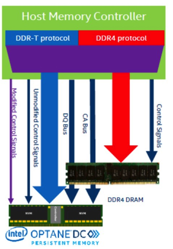
Note that almost all the same signals go to both the DDR4 DIMM and the “Intel Optane DC Persistent Memory” module – the only difference is the purple arrow on the far left labeled “Modified Control Signals.” These Modified Control Signals use a few pins that are not assigned on the JEDEC-standard DDR4 interface.
By doing this Intel alerted the industry of a problem that needs to be addressed when new memory types come to computing, and then provided one solution to that problem. Persistent memory can be attached directly to the processor as a DIMM (called “Near Memory”), or it can be managed in large pools that may reside off of the server motherboard (“Far Memory”). Intel’s solution for Far Memory is CXL, while for Near Memory the solution is DDR-T. But DDRT needs to be reconfigured every time the DDR interface is redefined, moving from DDR4 to DDR5, and then to DDR6 and beyond.
This problem was also identified by IBM, who developed the OpenCAPI standard, which includes the OMI memory interface that is explained in this white paper. CXL recently merged with OpenCAPI, and that indicates that OMI may become the industry-standard way of attaching any speed of near memory to the processor.
Managing Variable Memory Latency
For the past 50 years, computers have managed latency by breaking the system into 2 channels, the memory channel for low-latency access, and the I/O channel for everything else. The I/O uses interrupts and context switches to allow the processor to continue with other tasks while waiting for slow I/O. Processor context switches are time consuming since the processor must begin the context switch by pushing the program counter and various internal registers onto the stack, and end the context switch by popping them all back off the stack to restore the processor’s original state. Context switches can take about 100s to do all of this, and that’s about 3 orders of magnitude longer than Optane’s 100ns latency.
The diagram below, from SNIA, shows this relatively clearly. This chart plots the approximate latency of 4 storage device types on a logarithmic vertical scale. The colors on the chart’s background show 3 zones to indicate the latencies at which the context switch penalty can and cannot be tolerated. From 1.0E+4 to 1.0E+9 nanoseconds a context switch will add little enough to the latency that it will not be noticed, but in the green section at the lower part of the chart, at around 1.0E+2 nanoseconds and faster, a context switch adds an enormous burden to a transaction’s latency. In this faster zone it makes more sense for the CPU to wait for a transaction to complete by polling, or looping, until the transaction is through. In the middle, around 1.0E+3 nanoseconds, it’s hard to determine which approach is preferable.
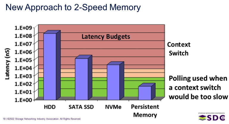
Note that until persistent memory was introduced all forms of persistent storage were slow enough to be managed with interrupts that would cause a context switch in the CPU. Optane changed all that to make polling a better choice for persistent memory. An interrupt structure would add three orders of magnitude to Optane’s latency, but since Optane is much slower than DRAM older systems would have no alternative.
Instead, Intel’s engineers brough back an old technique, polling, that had been abandoned long ago. Intel’s use of polling has opened designers’ eyes to a way to handle I/O that they had previously ignored, and this led to the development of high-speed CXL channels, CXL.mem and CXL.cache, that are designed to manage slower memory accesses that are not based on context switches.
Large Memory Expansion
As processor speeds increase the memory channel clock rate has tried to keep pace, making it unable to support more than two DIMMs per memory channel, since the capacitance of an additional DIMM would require the channel’s clock rate to be reduced. This puts a cap on the size of memory that can be attached to the processor.
There’s never enough memory bandwidth to support a ballooning number of cores, so processor designers have added memory channels, but each channel consumes more pins and more power, increasing the die size and cost, while robbing power that would otherwise be available to the processor cores.
Intel intended for Optane to help address this problem by creating a new way to increase the size of main memory, to support server users who wanted memories that were bigger than they could build using commonly-available DRAM DIMMs. To help that effort along the company set Optane prices at half the price of DRAMhttps://thememoryguy.com/intels-optane-dimm-price-model/. What’s not to like about more memory for less money?
But Optane requires a DDR-T, which adds Optane capabilities to the DDR4 bus. This posed a problem for Intel since the industry’s move to DDR5 required the development of a DDR5 version of DDR-T. Sometime after that it would need to do the same for DDR6 and future DDR generations.
Since large memories have become a concern, a number of companies developed various Far Memory approaches, including CXL, OpenCAPI, GenZ, and CCIX. All of these support larger memory pools than can be built out of standard DDR memory interfaces. For Intel, the use of one of these interfaces meant that they would no longer need to redesign DDR-T for every new generation of DDR.
All 4 of these interfaces share certain common goals, and that put them into competition with each other. As a result, they have been merging into CXL one by one to become a single standard. With CXL, a single processor can connect to very large memories via an interface that adds little latency, especially when compared to standard I/O.
The CXL spec is relatively new, but it has been evolving at a rapid pace. The recently-adopted CXL version 3.0, adds support for system architectures with multiple hosts sharing a memory space. This allows very large messages to be passed between processors at a much higher speed than could be achieved by passing them via shared storage.
The block diagram below shows how CXL 3.0 can connect eight hosts to each other, all sharing to two memory pools (labeled as “MC” on the right-hand side), via 4 switches.
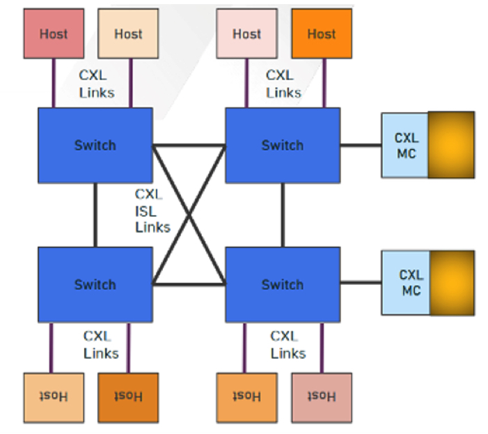
Configurations will naturally be found mainly in hyperscale computing systems, including leading Internet data centers, and those large computing installations dedicated to scientific processing, weather forecasts, and aerodynamics, and similar computationally-intense tasks.
The concept of large memory pools and shared memory stems from models developed for Optane, which led designers to consider how they could to expand memory without concerns about capacitive loading and pin count. System architects believe that the enormous memory size supported by CXL will more than offset the additional latency of the switching interface.
Addressing Persistent Memory Security Concerns
Security experts focus a good bit of attention on devices that store data and persistent memory falls into that category along with SSDs and HDDs. When such equipment is removed from a system due to failure or obsolescence, it might still contain sensitive data, and that data might be recovered by others for illicit use. DRAM never had this problem since its contents are lost once power is removed.
SSDs and HDDs have developed means to deal with this, and data can be destroyed in many ways:
- Physical destruction, crush or shred the device
- Secure erase software on the host or the SSD/HDD.
- If on the host it typically writes random data the device over and over.
- Internal device erases are triggered by a command from the host which causes the device to repeatedly erase and overwrite each track until power is removed.
- AES encryption, which encrypts the device’s contents. Data can only be deciphered using the encryption the key which must be kept in both the host and the device. Losing either causes the data to become illegible, and it takes very little time to destroy a key so that the device’s data is permanently lost.
Intel’s Optane DIMMs use the last approach, making the device the first DIMM ever to offer encryption.
Optane uses its AES encryption somewhat uniquely:
- In “Memory Mode”https://thessdguy.com/intels-optane-two-confusing-modes-part-2-memory-mode/ the Optane DIMM simply looks like an extremely large DRAM, and doesn’t offer persistence to the user. The DIMM’s drivers take advantage of that and pointedly lose Optane’s AES key whenever power is removed. Optane thus wakes up from a powered-down state with random contents.
- In “App Direct Mode”https://thessdguy.com/intels-optane-two-confusing-modes-part-3-app-direct-mode/, which offers users persistence, the data must be available after power is lost and restored again. To do this, Optane stores the encryption key on the module itself, which the host can access by using a passcode. The module’s contents can only be read by using the passcode.
Optane DIMMs provide additional security by also supporting the internal overwrite mechanism that, upon command, erases and over-writes all addresses.
At some time in the future persistent memory is certain to be reintroduced, and security issues will already have been and solved, thanks to the work done to support Optane’s security. This will help to accelerate the new memory’s adoption.
Summary
This article has detailed the 6 supporting technologies that were developed thanks to Intel’s introduction of Optane, many of which are likely to become a key part of all computing over time:
- A new programming paradigm
- Added processor instructions
- Handling 2-speed memory
- Managing variable memory latency
- Large memory expansion
- Addressing persistent memory security concerns
With Optane, Intel has given the industry these 6 new tools that we may not have otherwise had.


 Subscribe to our free daily newsletter

