


NAND Memories Before Flash?
Possible
This is a Press Release edited by StorageNewsletter.com on November 24, 2022 at 2:02 pm This report, published on October 28, 2022, was written by Jim Handy, semiconductor industry analyst, Objective Analysis.
NAND Memories Before Flash?
I wasn’t aware of any NAND memories prior to NAND flash, but recently learned that the idea wasn’t new, and other developments that enabled NAND flash were also developed before NAND flash memory was invented.
Although these ideas never reached commercial success the way that NAND flash did, they certainly made NAND flash possible.
The earlier device was an EPROM, which was the only reprogrammable nonvolatile memory from 1971 until EEPROM’s introduction in the 1974. EPROM remained the leading type of reprogrammable nonvolatile memory until NOR flash arrived in 1988. EPROM is very similar to flash since it uses a floating gate cell, but the only available erase mechanism for the floating gate was exposure to ultraviolet (UV) light until the development of the electrically-erasable EEPROM (or E²PROM). EPROMs shipped in packages with a transparent window over the chip.
EPROMs were produced with each bit connected to a wordline and a bitline in a configuration that was later named “NOR” to differentiate it from the new NAND approach that was first disclosed in a May 1986 paper: A High Density EPROM Cell and Array, presented at the IEEE Symposium on VLSI Technology by R. Stewart and others at the RCA David Sarnoff Research Center. In the NAND configuration a string of bits is run in series and only connects to the bitline at the end of the string.
This illustration shows the layout of the RCA part.
Stacked EPROM memory cells
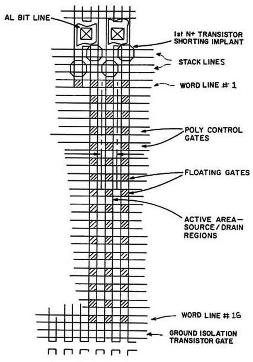
According to the paper this layout is “…not only smaller than existing EPROM cells but is even smaller than most existing mask programmable ROM cells.” This approach: “…could permit fabrication of VLSI EPROM’s with a lower cost/bit than mask programmable ROMs.”
An advantage the RCA design has over mask ROMs is that: “Elimination of the custom masks would make it easier to automate the wafer processing, would reduce inventory, and would permit redundant designs.” In other words, a single design could be used to store a number of programs, solving some of the key issues that faced mask ROM users.
The NAND EPROM’s programming technique had to be changed from that used in existing EPROMs. The researchers found that their small NAND cell was poorly suited to hot electron programming (“hot electron injection” or “hot carrier injection”) but was suitable for Fowler-Nordheim tunneling, so they adopted Fowler-Nordheim tunneling and abandoned the standard hot electron approach.
In the same way, today’s NOR flash is programmed using hot electron injection, and NAND flash is programmed with Fowler-Nordheim tunneling. This is the second invention from this paper that is still in use today.
According to the researchers, this was not the first use of NAND structure in a memory chip. The paper notes that “The EPROM array organization is similar to the dense NAND stacks arrays used in some ROM arrays.”
The authors don’t give further information about this NAND ROM, nor do they cite it in their references.
Something that bothers me a bit is a sentence towards the end of the paper: “The cells can be block erased with either UV light or by grounding the word lines with 17V applied to the bit lines.”
This sounds very similar to NAND flash memory. Is it possible that these RCA developers inadvertently invented NAND flash one year before Fujio Masuoka’s 1987 IEDM presentation of the chip that the industry calls the first NAND flash?
The RCA team appears not to have known about Masuoka’s original disclosure of the flash memory concept in his 1984 IEDM paper, though, since they say that “Electrical erase can be employed if necessary to eliminate expensive transparent lid packages.”
The fact that they didn’t mention flash implies that they were unaware of Masuoka’s 1984 presentation.
The RCA paper is an interesting piece of history that sheds a lot of light on the evolution of NAND flash. I was delighted to have been able to read it and to learn that certain advances were made much earlier than I originally thought.
The Memory Guy thanks Chris Burke of BTB Integrated Marketing for finding a pdf of the IEEE paper.


 Subscribe to our free daily newsletter

