Micron First to Market 232-Layer NAND
6th gen of NAND going into volume manufacturing
This is a Press Release edited by StorageNewsletter.com on August 3, 2022 at 2:02 pm By Lars Heineck, VP, advanced NAND technology, Micron Technology, Inc.
Lars Heineck shares insights into the development of Micron’s market-leading 232-layer 3D NAND technology.
 The semiconductor industry is interesting, but also unrelentingly challenging. The old saying that ‘it’s hard to work your way to the top, but it’s even harder to stay there’ is so very true. There is a constant pressure to push the bounds of physics, chemistry, manufacturing and innovation to deliver greater advances for computing devices – logic, memory, storage and more. Building technologies that are smaller, faster, less power-hungry and lower cost with greater capacity are challenges we grapple with daily. When we reach new levels with new technologies and first-to-market products, it’s an opportune time to reflect on our accomplishments.
The company has long been a recognized leader in 3D NAND technology, most recently evidenced by the ramp of our industry-first 176-layer replacement gate NAND technology. Since that time, we have demonstrated operational excellence by bringing that advanced technology broadly to market across our storage portfolio – mobile, client, automotive, intelligent edge and data center – and across a variety of form factors and interface technologies.
But even as we were perfecting and expanding implementations of 176-layer technologies, our team was also hard at work developing the next advancement in NAND. It was a moment of great pride for the team when Scott DeBoer and the Micron executive staff announced our next-generation 232-layer NAND technology, which is ramping into volume manufacturing through the end of 2022.
This announcement marks the debut of the industry’s first 232-layer 3D NAND, which is now shipping on selected Crucial-branded SSDs. Additional products based on this technology will ship later this year, offering high-capacity, higher-density storage with lower energy consumption and lower cost per bit.

Building up, not out
When discussing what we do with less technical audiences, I often see that they can comprehend the ‘more layers is better’ concept easily. So it’s good to share some nuance to this advancement and it’s impact with a broader audience.
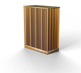
In the case of layers of 3D NAND, more is better. Think of a building in an overcrowded city where real estate is expensive: Expanding outward may not be possible or cost-effective ways to increase density to support population growth. In many cities, the alternative is to grow upward by adding skyscrapers and apartment buildings with more levels and units in the same space. This approach allows for much higher occupancy rates. Similarly, parking spaces and infrastructure for the building’s water and HVAC would largely be located under the building for greater space efficiency.
232-layer design builds on our successful and proven CMOS under array (CuA) architecture that provides a scale-up approach for capacity growth, density, performance, and cost improvements. Stacking the bit cell array of the NAND into more layers provides more bits per square millimeter of silicon, allowing greater density and lower cost per bit.
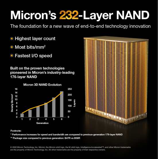
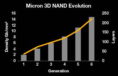
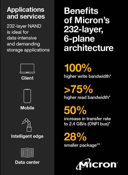
This first-to-market 232-layer technology represents the company’s 6th generation of NAND going into high-volume manufacturing. The breakthrough high layer count, along with CuA technology, allows us to deliver huge storage capacity up to 1Tb per chip on a very small footprint. As a result, the bit density per area on the 232-layer NAND device is over 45% higher than that for the previous 176-layer generation, an amazing increase in capability. The increase in density also enables improved form factor packages, such as the new 11.5×13.5mm package, which is 28% smaller than the packages for previous-gen chips. All this means that more types of devices can now be equipped with large capacity, high-performance storage.
Featuring more performance, better QoS
Increased density is just the beginning. Besides having the most layers in the industry, the 232-layer NAND is also the fastest. One factor is an increased open NAND flash interface (ONFI) transfer rate of 2400MT/s, again leading the industry. That’s 50% faster than previous-generation technology. Bandwidth has also improved in both directions, with up to 100% higher write bandwidth and greater than 75% higher read bandwidth compared to previous generation 176-layer NAND.
Making this improved storage and performance accessible required increasing the partitioning of the 3D NAND devices into 6 planes to achieve higher degrees of parallelism that contribute to the performance increase. Many NAND devices in the market today only feature 2 planes. While even the current leading-edge designs feature 4 planar partitions to channel commands and data flows, we are bringing the first 6-plane TLC NAND device to the market.
On a per-die basis, the increased parallelism improves both read and write performance for sequential and random access by enabling more read and write commands that can be issued to the NAND device simultaneously. As a result, the 6-plane architecture, along with the corresponding number of independent wordlines of our new 232-layer NAND, also improves QoS by reducing the number of collisions between read and write commands. Much like a freeway, more lanes lead to less congestion and better traffic flow through a given area.
Conquering new heights
While simply adding more layers to 3D NAND flash should be a breeze, it’s not. These devices can be challenging to fabricate, requiring many hundreds of individual processes to take a raw wafer through to completed dies, or chips.
Perhaps the biggest challenge with stacking layers higher is the difficulty in ensuring uniform construction up and down the stack – but this uniform construction is essential to properly aligning all the layers and connecting pillars.
Consider just these few examples of the challenges, though there are more:
- The reduced distance between the vertical wordline layers comes with higher cell-to-cell capacitive coupling, which needs to be overcome.
- Process challenges for pillar-etch functions multiply quickly due to the higher layer count.
The company uses advanced etching and patterning techniques to create the high aspect ratio structures, as well as a highly effective replacement gate process to improve the part’s performance.
‘Team building’
Meeting these challenges requires tightly aligned teams that represent design, technology development, system enablement, wafer manufacturing, test and packaging, as well as many other supporting functions. Optimizing these cross-functional teams is the key to success in building such complex solutions. From a design and technology co-optimization perspective, it’s important to understand what the process effects are and how to adjust the design to be more robust. For example, 3D NAND needs advanced data management and error correction from its controllers to increase program cycles. Accurate floor planning and modeling are important to ensure that electrical, power and thermal specifications can reliably be met due to process variations.
While it is indeed difficult to prototype an innovative semiconductor design, it’s an even greater challenge to ramp 3D NAND into high-volume manufacturing. 3D NAND cells are built vertically as strings, so a defect in a single cell can affect the performance of a cell string. Extreme precision is required for high aspect ratio etching features, addressing advanced contamination control to reduce defects while boosting electron mobility and conductivity to address slowdown issues.
While Micron has in-house expertise to drive this innovation, we also work in collaboration with our manufacturing OEM vendors, material makers, and suppliers to develop solutions to precisely construct memory cells in extreme geometries.
Coming soon to an SSD near you
The 232-layer NAND represents a watershed moment for the continued digitization of life from the device to the intelligent edge to the cloud. From the ability to support camera technology in the earliest cell phones to the introduction of tablets, thin and light laptops, and wearables, solid-state storage technology has been a key enabler in the evolution of technology. Without the ability to store applications and data, the evolution of technology is greatly hampered.
Our teams like the description of ‘first to market, second to none’ as it reflects our commitment to leadership. With each successive advancement in layer count, Micron delivers increased storage density, improvement in energy efficiency and lower cost per bit. These improvements help unlock new opportunities for digitization, optimization and automation. The company maintains technology leadership by continuously pushing the envelope in design, process and manufacturing excellence. We have raised the bar with this technology and look forward to seeing the wave of new product innovation that this technology will unlock.
Resources :
Micron 232-layer NAND technology
Video: Micron NAND Technology: Innovation and Leadership Extended
Video: Jeremy Werner, CVP and GM, Micron, and Bill Cerreta, VP and GM, Pure Storage, sat down with industry analyst, Patrick Moorhead, to talk about Micron’s new 232-layer NAND


 Subscribe to our free daily newsletter


