Why USA Needs CHIPS Act?
Open letter from Nantero CEO
This is a Press Release edited by StorageNewsletter.com on July 29, 2022 at 2:02 pm![]() By Rob Snowberger, CEO, Nantero, Inc.
By Rob Snowberger, CEO, Nantero, Inc.
We commend the United States Senate for their 63-34 vote on July 19, 2022 confirming the Motion to Proceed to the House Message to Accompany H.R. 4346. This important step sets in motion the procedure to pass the legislation known as the CHIPS Act, which the company supports as it is essential to American competitiveness and national security. The CHIPS Act and associated funding will strengthen our domestic semiconductor industry and repatriate the ability for breakthrough technologies to make it through the financial ‘Valley of Death’ and onto commercial markets without having to make the decision to leave U.S. shores. The economic power and job creation that will come from this decision will impact not only the needs of current citizens of USA, but also buttress the financial independence and security of generations to come.
Most Americans are likely not familiar with the massive costs and monopolistic nature of the semiconductor business. They are also likely not aware that ‘tech’ companies like Google, Apple, Facebook, and Twitter are not semiconductor companies. What most Americans likely are familiar with are the various benefits and importance of semiconductors, as they are the heart of many electronic components within our smartphones, computers, cars, homes, and virtually everything in our modern lives (as well as our tanks, fighter jets and critical infrastructure). However, even with this limited understanding around the role of semiconductors, the general public does not often see the critical need for this legislation. In contrast, a company such as Nantero has had a 20-year front row seat to the daily struggle as a US-based semiconductor ‘start-up’ company. As a result, we know that this legislation is not only needed, but critical to helping technologies that are invented in the U.S. stay and benefit the U.S.
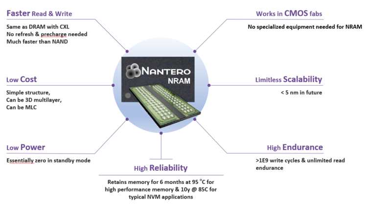
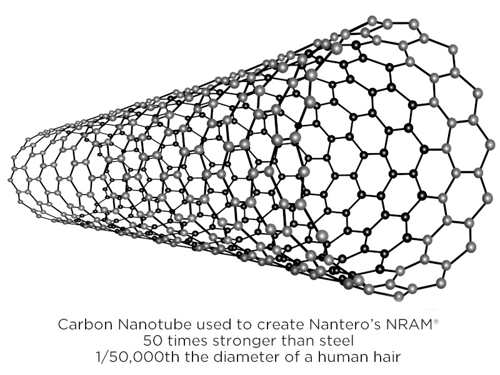
The flagship of Nantero’s business is its memory device called NRAM (Non-volatile Random Access Memory). NRAM utilizes a carbon nanotube technology (CNT) lattice as the switching mechanism within our memory cell, allowing it to achieve non-volatility in main memory at the same performance and speed of DRAM (which, of course is volatile). While development costs and fab access constraints have defined Nantero’s ‘David and Goliath’ struggle with DRAM, we have an extremely viable roadmap that is cost competitive with DRAM within 2 years from the production of our first 16Gb (12nm) DDR5 chip. Additionally, we are designing for the CXL architecture which makes NRAM an attractive next-gen memory technology for embedded applications. And more importantly, we have recently achieved 5-sigma on 1T1R memory 300mm wafers (55nm) at 1 million cycles for a product we are pursuing with Fujitsu Ltd. out of the former USJC fab in Japan. This is a milestone in proving the manufacturability of our CNT-based memory.
While the company was born within an U.S. research institution (Harvard) and nursed within the robust U.S. venture capital markets, it is at risk of being lost overseas at the exact moment our technology is ready to impact the US economy. In fact, NRAM is within that particular ‘ripened’ moment in its technology lifecycle where nation-state-backed funding has historically been deployed to propel proven technologies out of the ‘Valley of Death’ and into a successful, world-changing commercial industry that is a source of national pride. For NRAM and Nantero, this moment simply seems to be drifting toward Japan as many Japanese industry giants and the Japanese government have recognized the extremely strong value proposition of NRAM and have recently invested heavily in the technology.
The company’s story as described above is commonplace in the U.S. semiconductor industry, and it costs the U.S. trillions of dollars in economic benefit and national security concerns each year. The CHIPS Act is America’s response to these foreign sovereign funds who have been investing in this process for decades, and Nantero is in full support. We applaud the Senate for taking this important step.
Very respectfully,
Rob Snowberger, CEO, Nantero
Comments
Some Nantero’s USPTO patents:
Accessing resistive change elements in resistive change element arrays
Nantero, Inc., Woburn, MA, has been assigned a patent (11,393,508) developed by Luo, Jia, Fremont, CA, for "methods for accessing resistive change elements in resistive change element arrays."
The abstract of the patent published by the U.S. Patent and Trademark Office states: "Devices and methods for accessing resistive change elements in a resistive change element array to determine resistive states of the resistive change elements are disclosed. According to some aspects of the present disclosure the devices and methods access resistive change elements in a resistive change element array through a variety of operations. According to some aspects of the present disclosure the devices and methods supply an amount of current tailored for a particular operation. According to some aspects of the present disclosure the devices and methods compensate for circuit conditions of a resistive change element array by adjusting an amount of current tailored for a particular operation to compensate for circuit conditions of the resistive change element array.”
The patent application was filed on May 10, 2019 (16/409,611).
Electrostatic discharge protection devices using carbon-based diodes
Nantero, Inc., Woburn, MA, has been assigned a patent (11,387,277) developed by Bertin, Claude L., Venice, FL, Rueckes, Thomas, Byfield, MA, Huang, X. M. Henry, Cupertino, CA, and Cleavelin, C. Rinn, Lubbock, TX, for an "electrostatic discharge protection devices using carbon-based diodes."
The abstract of the patent published by the U.S. Patent and Trademark Office states: "The present disclosure is directed toward carbon based diodes, carbon based resistive change memory elements, resistive change memory having resistive change memory elements and carbon based diodes, methods of making carbon based diodes, methods of making resistive change memory elements having carbon based diodes, and methods of making resistive change memory having resistive change memory elements having carbons based diodes. The carbon based diodes can be any suitable type of diode that can be formed using carbon allotropes, such as semiconducting single wall carbon nanotubes, s-SWCNT, semiconducting Buckminsterfullerenes, such as C60 Buckyballs, or semiconducting graphitic layers (layered graphene). The carbon based diodes can be pn junction diodes, Schottky diodes, other any other type of diode formed using a carbon allotrope. The carbon based diodes can be placed at any level of integration in a three dimensional (3D) electronic device such as integrated with components or wiring layers.”
The patent application was filed on June 29, 2020 (16/915,414).
Combinational resistive change elements
Nantero, Inc., Woburn, MA, has been assigned a patent (11,295,810) developed by Luo, Jia, Fremont, CA, Cleveland, Lee E., and Chan, Ton Yan Tony, Santa Clara, CA, for "combinational resistive change elements."
The abstract of the patent published by the U.S. Patent and Trademark Office states: "Combinations of resistive change elements and resistive change element arrays thereof are described. Combinational resistive change elements and combinational resistive change element arrays thereof are described. Devices and methods for programming and accessing combinations of resistive change elements are described. Devices and methods for programming and accessing combinational resistive change elements are described.”
The patent application was filed on June 7, 2019 (16/434,813).
Resistive change elements using passivating interface gaps and methods for making same
Nantero, Inc., Woburn, MA, has been assigned a patent (11,258,023) developed by Ramsbey, Mark, Sunnyvale, CA, Rueckes, Thomas, Byfield, MA, Yamaguchi, Tatsuya, Nozawa, Syuji, Yamanashi, Japan, and Sato, Nagisa, Tokyo, Japan, for "resistive change elements using passivating interface gaps and methods for making same."
The abstract of the patent published by the U.S. Patent and Trademark Office states: "A method to fabricate a resistive change element. The method may include forming a stack over a substrate. The stack may include a conductive material, a resistive change material, a first surface, and a second surfaces opposite the first surface. The method may further include depositing a first material over the stack such that the first material directly contacts at least one of the first surface and the second surface of the stack. The method may also include after depositing the first material, forming a second material over the first material and evaporating a portion of the first material through the second material to create a gap between the second material and the at least one of the first surface and the second surface of the stack.”
The patent application was filed on August 5, 2020 (16/985,657).
Nonvolatile nanotube switch elements using sidewall contacts
Nantero, Inc., Woburn, MA, has been assigned a patent (11,177,261) developed by Bertin, Claude L., Venice, FL, Rueckes, Thomas, Byfield, MA, Huang, X. M. Henry, Cupertino, CA, Sivarajan, Ramesh, Shrewsbury, MA, Ghenciu, Eliodor G., Atherton, CA, Konsek, Steven L., Boston, MA, and Meinhold, Mitchell, Arlington, MA, for a "nonvolatile nanotube switch elements using sidewall contacts."
The abstract of the patent published by the U.S. Patent and Trademark Office states: "Under one aspect, a non-volatile nanotube diode device includes first and second terminals, a semiconductor element including a cathode and an anode, and capable of forming a conductive pathway between the cathode and anode in response to electrical stimulus applied to the first conductive terminal, and a nanotube switching element including a nanotube fabric article in electrical communication with the semiconductive element, the nanotube fabric article disposed between and capable of forming a conductive pathway between the semiconductor element and the second terminal, wherein electrical stimuli on the first and second terminals causes a plurality of logic states.”
The patent application was filed on January 27, 2020 (16/752,861).
Storage and delivery systems for colloidal dispersions
Nantero, Inc., Woburn, MA, has been assigned a patent (11,117,289) developed by Smith, Billy, Woburn, MA, Cook, David, Salem, NH, Roberts, David A., Woburn, MA, and Bengtson, Thomas R., Derry, NH, for "storage and delivery systems for colloidal dispersions."
The abstract of the patent published by the U.S. Patent and Trademark Office states: "The present disclosure provides methods for stabilizing a colloidal dispersion during transport for low defect tolerance applications. The methods involve eliminating fluid interfaces within a dispersion, storing the dispersion in an environment of inert gas, and degassing the dispersion. Several bottle closure devices are described which may be ideal for use with these methods, being able to seal a container filled with a dispersion, permit the removal of headspace and rapidly empty the contained dispersion. In one aspect, the device includes a vented cap and semi-permeable membrane, which allows the passage of gas into and out of the container, and a dispenser nozzle integrated with the device to allow a stored dispersion to be dispensed without removing the device from the container. In another aspect, the bottle closure device includes an attachment point for a removable downtube and dispenser nozzle.”
The patent application was filed on July 19, 2017 (15/653,808).
Nanotube solution treated with molecular additive, nanotube film having enhanced adhesion property, and methods for forming nanotube solution and nanotube film
Nantero, Inc., Woburn, MA, has been assigned a patent (11,072,714) developed by Roberts, David A., Woburn, MA, Sen, Rahul, Lexington, MA, Sites, Peter, Marblehead, MA, Kocab, J. Thomas, Exeter, RI, and Gu, Feng, Ellicot City, MD, for "nanotube solution treated with molecular additive, nanotube film having enhanced adhesion property, and methods for forming the nanotube solution and the nanotube film."
The abstract of the patent published by the U.S. Patent and Trademark Office states: "The present disclosure provides a nanotube solution being treated with a molecular additive, a nanotube film having enhanced adhesion property due to the treatment of the molecular additive, and methods for forming the nanotube solution and the nanotube film. The nanotube solution includes a liquid medium, nanotubes in the liquid medium, and a molecular additive in the liquid medium, wherein the molecular additive includes molecules that provide source elements for forming a group IV oxide within the nanotube solution. The molecular additive can introduce silicon (Si) and/or germanium (Ge) in the liquid medium, such that nominal silicon and/or germanium concentrations of the nanotube solution ranges from about 5 ppm to about 60 ppm.”
The patent application was filed on April 24, 2017 (15/495,170).
Devices for programming resistive change elements in resistive change element arrays
Nantero, Inc., Woburn, MA, has been assigned a patent (11,037,624) developed by Luo, Jia, Fremont, CA, Ning, Sheyang, Milpitas, CA, and Cleveland, Lee E., Santa Clara, CA, for "devices for programming resistive change elements in resistive change element arrays."
The abstract of the patent published by the U.S. Patent and Trademark Office states: "Devices and methods for programming resistive change elements using an electrical stimulus are disclosed. According to some aspects of the present disclosure the devices and methods program at least one resistive change element within at least one resistive change element cell in a resistive change element array using an electrical stimulus having a voltage level greater than a steady state voltage level that can be supplied by a power supply.”
The patent application was filed on October 11, 2019 (16/600,025).
Complete list of Nantero’s USPTO patents


 Subscribe to our free daily newsletter


