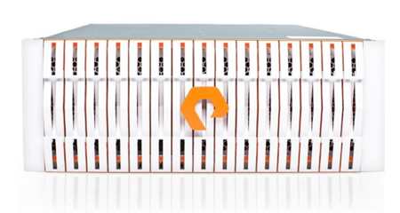
Pure Storage FlashBlade Solution
Accelerates time-to-market for electronic design automation workloads.
This is a Press Release edited by StorageNewsletter.com on May 9, 2022 at 2:00 pmPure Storage, Inc. is empowering electronic design automation (EDA) workloads and accelerating next-gen chip design.
Modern EDA chip development requires performance storage that can serve thousands of powerful servers and fast networks in all dimensions of concurrency – throughput, IO/s, latency, fast deletes, capacity and metadata – to eliminate bottlenecks that slow data access. While legacy storage architectures add unnecessary complexity and either saturate or scale inefficiently when faced with modern EDA workloads, FlashBlade was designed to meet the high-concurrency requirements of semiconductor and EDA workloads. As a result, 50% of the top 10 semiconductor companies rely on the solution to remain competitive and expedite time to market.
By consolidating two traditionally separate storage paradigms – file and object storage- into one performant data solution, FlashBlade enables organisations to replace siloed collections of data with a single scale-out storage solution that delivers multidimensional performance at scale. This combination of file and object storage protocols with the low latency, massive parallelism, and high throughput capabilities of enterprise all flash storage, make it a storage solution for EDA workloads.
The firm is continuing to grow its EDA footprint with more companies now using FlashBlade for analytics and technical computing to expedite modern chip design processes as their chip design business units grow rapidly. In fact, software developers are seeing workloads finish more than 5x faster than the status quo with FlashBlade and benefiting from up to 2.5:1 data reduction through compression.
Customer examples include:
-
Company in the semiconductor industry that leverages FlashBlade’s performance and stability for Rapid Restore to maintain a more stable production line, a fast development cycle, and a cost-effective development environment through data reduction.
-
Electronics and smart home technology company is using FlashBlade to finish more EDA jobs and bring chip design to market faster. Furthermore, performance at scale with minimal intervention enables smoother management and frees up staff for other tasks.
-
Multinational semiconductor, software and wireless technology company cites FlashBlade for helping the company reach its Capex and Opex goals with simplified management and performance capable of meeting the demands of modern unstructured data that EDA workloads require.
-
Another FlashBlade EDA customer creating chip design software reported a greater than 10x improvement in run time of its highly concurrent software build and regression workload – with runtimes repeatedly decreasing from 6 hours to 20 minutes.
FlashBlade’s performance and scalability are driving tomorrow’s next-gen chip designs and its ability to scale IO efficiently under massive parallelism is making an impact on semiconductor designers globally. By speeding up all aspects of the design flow – from RTL design to tapeout – FlashBlade helps customers release products faster, with higher quality and lower cost, and improves engineering productivity with the ability to do more designs at the same time. Additionally, customers can take advantage of FlashBlade at Equinix with Microsoft Azure for EDA, to leverage cloud-adjacent storage for EDA workloads.


 Subscribe to our free daily newsletter


