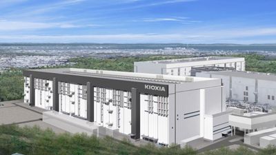
Kioxia Debuts Construction of Yokkaichi Plant in Mie Prefecture, Japan
For sixth-gen 3D flash memory production with WD
This is a Press Release edited by StorageNewsletter.com on March 4, 2021 at 2:16 pmKioxia Corporation held a groundbreaking ceremony for its semiconductor fabrication facility (Fab7) at Yokkaichi Plant in Mie Prefecture, Japan.

The facility will be an advanced manufacturing operations, dedicated to production of its proprietary 3D flash memory BiCS flash. The first phase of construction is scheduled to be completed by the spring of 2022. Construction of the facility will be divided into 2 phases to allow for continued production and shipment of flash memory products to meet ongoing market demand.
The Fab7 facility will have an earthquake absorbing structure and an environmentally friendly design that includes energy saving manufacturing equipment. Located in Yokkaichi Plant, which offers the world’s largest flash memory production capacity, the Fab7 facility will boost firm’s entire production capacity by introducing an manufacturing system that utilizes AI.
Consistent with Kioxia’s 20-year partnership with Western Digital Corporation, the 2 companies regularly collaborate on facility operation. Accordingly, they expect to continue their joint venture investments for the Fab7 facility, including the creation of sixth-gen 3D flash memory.
Due to technological innovations, the amount of data being generated, stored and used around the world has increased. The flash memory market expects further growth driven by cloud services, 5G, IoT, AI and automated driving. As a result, the production in Fab7 facility will continue to meet the increasing demand for memory.


 Subscribe to our free daily newsletter

