Why 3D NAND Stuck at 40nm?
How much 3D NAND pitches had shrunk since the technology's 2013 introduction?
This is a Press Release edited by StorageNewsletter.com on November 12, 2020 at 2:38 pm![]() This is an interview with analyst Jim Handy, coming to Objective Analysis with over 30 years in the electronics industry including 14 years as an industry analyst for Dataquest (now Gartner) and Semico Research.
This is an interview with analyst Jim Handy, coming to Objective Analysis with over 30 years in the electronics industry including 14 years as an industry analyst for Dataquest (now Gartner) and Semico Research.
You wrote a blog post about 3D NAND saying that it couldn’t scale. Why did you write that?
Someone asked me how much 3D NAND pitches had shrunk since the technology’s 2013 introduction, since Samsung made said back in 2015 that they used 40nm. Nobody had given an update since then. It seemed like it should have migrated to smaller processes like 35nm, 25nm, and 20nm. I replied in my blog The Memory Guy that it’s nearly impossible to shrink the pitch of 3D NAND, at least not much. This is because of the way that it’s made.
Can you explain?
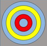
3D NAND is made by filling holes with a lot of layers of material. These layers determine the minimum diameter of the hole.Toshiba’s original BiCS structure is simpler than most processes, so I will use that to explain. The post used a conceptual drawing of one of the 3D NAND’s vertical strings viewed from the top to help explain.

Here’s how they make a vertical 3D NAND flash string:
- 1 First they etch deep narrow holes through all of the 3D NAND’s layers. Today these holes have aspect ratios of about 60:1. It’s like a well that’s 1 meter in diameter and 60 meters deep. It’s like that, with almost perfectly parallel walls for the entire depth of the well.
- 2 After that they precisely apply five very thin coatings to the walls of the hole:
- 1. The first is silicon dioxide (SiO2) which must be deposited accurately to the entire surface, and this makes the hole thinner. This is the gate oxide and is the pale blue ring in the sketch.
- 2. After this comes silicon nitride (Si3N4), which makes the hole even thinner. This is shown in yellow. It’s the charge trapping layerhttps://thememoryguy.com/the-invention-of-charge-trap-memory/.
- 3. Then a layer of SiO2 (blue) is applied and that makes the hole even thinner.
- 4. After that conductive polysilicon (red) is applied, to make the hole thinner yet. This is the channel.
- 5. By now the hole has gotten very tiny, and that’s filled with SiO2 (blue). This layer thins the channel to make it perform better.
And these layers are all very thin?
They are not only thin, but all of them must be uniform from top to bottom or the whole string will fail to work.
And you say they determine the minimum diameter of the hole.
The thickness of the layers that line the hole determines the diameter of the hole, and that limits how tightly the holes can be packed. The layers are about as thin as they can be made, and are a few atoms thick.
So you’re saying that 3D NAND can’t scale the way that planar NAND used to?
3D NAND will remain at 40nm for a long time. NAND no longer uses pitch scaling. R&D now focuses on layer count, logic-under-array, and better staircase configurations.


 Subscribe to our free daily newsletter

