R&D: From EPFL, Next-Gen Computer Chip With 2 Heads to Combines 2 Functions, Logic Operations and Storage
Technology is first to use 2D material for what’s called logic-in-memory architecture, or single architecture.
This is a Press Release edited by StorageNewsletter.com on November 9, 2020 at 2:05 pmBy Sarah Perrin, École Polytechnique Fédérale de Lausanne (EPFL)
EPFL engineers have developed a computer chip that combines two functions – logic operations and data storage – into a single architecture, paving the way to more efficient devices. Their technology is particularly promising for applications relying on AI.
It’s a breakthrough in the field of electronics. Engineers at EPFL’s Laboratory of Nanoscale Electronics and Structures (LANES) have developed a next-gen circuit that allows for smaller, faster and more energy-efficient devices – which would have major benefits for AI systems. Their technology uses a 2D material for what’s called a logic-in-memory architecture, or a single architecture that combines logic operations with a memory function. The research team’s findings appear in Nature.
Until now, the energy efficiency of computer chips has been limited by the von Neumann architecture they currently use, where data processing and storage take place in two separate units. That means data must constantly be transferred between the 2 units, using up a considerable amount of time and energy.
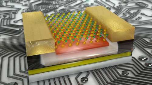
By combining the 2 units into a single structure, engineers can reduce these losses. That’s the idea behind the new chip developed at EPFL, although it goes one step beyond existing logic-in-memory devices. The EPFL chip is made from MoS2, which is a 2D material consisting of a single layer that’s 3 atoms thick. It’s also an excellent semi-conductor. LANES engineers had already studied the specific properties of MoS2 a few years ago, finding that it is particularly suited to electronics applications. Now the team has taken that initial research further to create their next-gen technology.
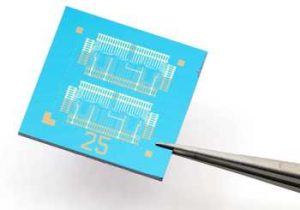
Computer chip that combines 2 functions – logic operations and data storage.
(© 2020 EPFL/LANES)
The EPFL chip is based on floating-gate field-effect transistors (FGFETs). The advantage of these transistors is that they can hold electric charges for long periods; they are typically used in flash memory systems for cameras, smartphones and computers. The unique electrical proprieties of MoS2 make it particularly sensitive to charges stored in FGFETs, which is what enabled the LANES engineers to develop circuits that work as both memory storage units and programmable transistors. By using MoS2, they were able to incorporate numerous processing functions into a single circuit and then change them as desired.
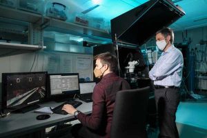
Guilherme Migliato Marega, lead author, and Andras Kis, LANES director
(© 2020 EPFL / A.Herzog)
In-depth expertise
“This ability for circuits to perform two functions is similar to how the human brain works, where neurons are involved in both storing memories and conducting mental calculations,” says Kis. “Our circuit design has several advantages. It can reduce the energy loss associated with transferring data between memory units and processors, cut the amount of time needed for computing operations and shrink the amount of space required. That opens the door to devices that are smaller, more powerful and more energy efficient.”
The LANES research team has also acquired expertise in fabricating circuits out of 2D materials.
“We made our first chip ten years ago by hand,” says Kis. “But we have since developed an advanced fabrication process that lets us make 80 or more chips in a single run, with well-controlled properties.”
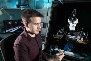
Guilherme Migliato Marega, lead author
(© 2020 EPFL / A.Herzog)
Article: Logic-in-memory based on an atomically thin semiconductor
Nature as published an article written by Guilherme Migliato Marega, Yanfei Zhao, Ahmet Avsar, Zhenyu Wang, Mukesh Tripathi, Electrical Engineering Institute, École Polytechnique Fédérale de Lausanne (EPFL), Lausanne, Switzerland, and Institute of Materials Science and Engineering, École Polytechnique Fédérale de Lausanne (EPFL), Lausanne, Switzerland, Aleksandra Radenovic, Institute of Bioengineering, École Polytechnique Fédérale de Lausanne (EPFL), Lausanne, Switzerland, Andras Kis, Electrical Engineering Institute, École Polytechnique Fédérale de Lausanne (EPFL), Lausanne, Switzerland, and Institute of Materials Science and Engineering, École Polytechnique Fédérale de Lausanne (EPFL), Lausanne, Switzerland.
Abstract: “The growing importance of applications based on machine learning is driving the need to develop dedicated, energy-efficient electronic hardware. Compared with von Neumann architectures, which have separate processing and storage units, brain-inspired in-memory computing uses the same basic device structure for logic operations and data storage1,2,3, thus promising to reduce the energy cost of data-centred computing substantially4. Although there is ample research focused on exploring new device architectures, the engineering of material platforms suitable for such device designs remains a challenge. Two-dimensional materials5,6 such as semiconducting molybdenum disulphide, MoS2, could be promising candidates for such platforms thanks to their exceptional electrical and mechanical properties7,8,9. Here we report our exploration of large-area MoS2 as an active channel material for developing logic-in-memory devices and circuits based on floating-gate field-effect transistors (FGFETs). The conductance of our FGFETs can be precisely and continuously tuned, allowing us to use them as building blocks for reconfigurable logic circuits in which logic operations can be directly performed using the memory elements. After demonstrating a programmable NOR gate, we show that this design can be simply extended to implement more complex programmable logic and a functionally complete set of operations. Our findings highlight the potential of atomically thin semiconductors for the development of next-generation low-power electronics.“


 Subscribe to our free daily newsletter


