R&D: Ultra-Fast Laser-Based Writing of Data to Storage Devices
Advancement for augmenting future storage devices
This is a Press Release edited by StorageNewsletter.com on August 20, 2020 at 2:06 pmFrom Eindhoven University of Technology
Researchers show that laser pulses can accurately and quickly change spin states in magnetic materials for future data storage needs.
Modern life revolves around data, which means that we need new, fast, and energy-efficient methods to read and write data on our storage devices. Optical-based approaches, which use laser pulses to write data instead of magnets, have received considerable attention over the past decade following the development of all-optical switching (AOS) for magnetic materials. While fast and energy efficient, AOS has issues with precision. Researchers at Eindhoven University of Technology have devised a new method to accurately write data to a cobalt-gadolinium (Co/Gd) layer with a laser pulse using a ferromagnetic material as a reference to help with the writing process. Their research is published in Nature Communications.
Magnetic materials in hard drives and other devices store data as computer bits, i.e. 0s and 1s, in magnetic spins orientated either up or down. Traditionally, data is read from and written to a hard drive by moving a small magnet over the material. However, with the demand for data production, consumption, access, and storage continually increasing, there is considerable demand for faster and more energy-efficient methods to access, store, and record data.
Need for deterministic single pulse AOS
All-optical switching (AOS) of magnetic materials is a promising approach in terms of speed and energy efficiency. AOS uses femtosecond laser pulses to switch the orientation of magnetic spins at the picosecond scale. Two mechanisms can be used to write data: multiple pulse and single pulse switching. In multiple pulse switching, the final orientation of the spins (i.e, up or down) is deterministic, meaning it can be determined in advance by the polarization of the light. However, this mechanism typically requires multiple lasers, which slows the speed and efficiency of writing.
On the other hand, a single pulse for writing would be much faster, but studies on single pulse AOS show that switching is a toggle process. This means that to change the state of a specific magnetic bit, prior knowledge of the bit is needed. In other words, the state of the bit must be read first before it can be overwritten, which introduces a read stage to the writing process, and thus limits speed.
A better approach would be a deterministic single pulse AOS approach, where the final direction of a bit depends only on the process used to set and reset the bit. Now, researchers from the Physics of Nanostructures group in the Department of Applied Physics at TU/e have demonstrated a new approach that can achieve deterministic single pulse writing in magnetic storage materials, making the writing process much more accurate.
Importance of reference and spacer layers
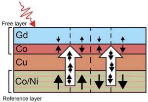
For their experiments, the TU/e researchers designed a writing system consisting of three layers – a ferromagnetic reference layer made from cobalt and nickel that assists or prevents spin switching in the free layer, a conductive copper (Cu) spacer or gap layer, and an optically switchable Co/Gd free layer. The thickness of the combined layers is less than 15 nm.
Once excited by a femtosecond laser, the reference layer demagnetizes in less than a picosecond. Some of the lost angular momentum associated with the spins in the reference layer is then converted into a spin current carried by electrons. The spins in the current are aligned with the spin orientation in the reference layer.
This spin current then moves from the reference layer through the Cu spacer layer (see white arrows in the image) to the free layer where it can assist or prevent spin switching in the free layer. This depends on the relative spin orientation of the reference and free layers.
Varying the laser energy leads to two regimes. First, above one threshold, the final spin orientations in the free layer are entirely determined by the reference layer, and second, above a higher threshold, toggle switching is observed. The researchers have shown that together these two regimes can be used for accurate writing of the spin states in the free layer without accounting for its initial state during the writing process. This finding presents an important advancement for augmenting our future data storage devices.
Full paper: Y.L.W. van Hees et al., Deterministic all-optical magnetization writing facilitated by non-local transfer of spin angular momentum, Nature Communications, (2020).
Article: Deterministic all-optical magnetization writing facilitated by non-local transfer of spin angular momentum
Nature Communications has published an article written by Youri L. W. van Hees, Paul van de Meugheuvel, Bert Koopmans, and Reinoud Lavrijsen, Department of Applied Physics, Institute for Photonic Integration, Eindhoven University of Technology, P.O. Box 513, 5600, MB, Eindhoven, the Netherlands.
Abstract: “Ever since its discovery around a decade ago, all-optical magnetization switching (AOS) using femtosecond laser pulses has shown potential for future data storage and logic devices. In particular, single pulse helicity independent AOS in certain ferrimagnetic alloys and multilayers is highly efficient and ultrafast. However, in most cases it is a toggle mechanism, which is not desirable for applications. Here we experimentally demonstrate conversion from toggle switching to a deterministic mechanism by biasing AOS in a Co/Gd bilayer with a spin polarized current which is optically generated in an adjacent ferromagnetic reference layer. We show deterministic writing of an ‘up’ and ‘down’ state using a sequence of one or two pulses, respectively, and demonstrate the non-local origin by varying the magnitude of the generated spin current. Our demonstration of deterministic magnetization writing could provide an essential step towards the implementation of future optically addressable spintronic memory devices.“


 Subscribe to our free daily newsletter


