









R&D: Stanford-led Team Shows How to Store Data Using 2D Materials Instead of Silicon Chips
Way to slide atomically-thin layers of 2D materials over 1D another to store more data, in less space and energy
This is a Press Release edited by StorageNewsletter.com on July 6, 2020 at 2:18 pmBy Andrew Myers, Stanford University
A Stanford-led team has invented a way to store data by sliding atomically thin layers of metal over one another, an approach that could pack more data into less space than silicon chips, while also using less energy.
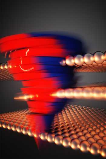
This illustrates how an experimental memory technology stores data by shifting the relative position of three atomically thin layers of metal, depicted as gold balls. The swirling colors reveal how a shift in the middle layer affects the motion of electrons in a way that encodes digital ones and zeroes.
(Image credit: Ella Maru Studios)
The research, led by Aaron Lindenberg, associate professor, materials science and engineering, Stanford University, and SLAC National Accelerator Laboratory, would be a significant upgrade from the type of nonvolatile memory storage that today’s computers accomplish with silicon-based technologies like flash chips.
Xiang Zhang, mechanical engineer, UC Berkeley, Xiaofeng Qian, materials scientist, TX A&M, and Thomas Devereaux, professor, materials science and engineering, Stanford/SLAC, also helped direct the experiments, which are described in the journal. The breakthrough is based on a newly discovered class of metals that form incredibly thin layers, in this case just three atoms thick. The researchers stacked these layers, made from a metal known as tungsten ditelluride, like a nanoscale deck of cards. By injecting a tiny bit of electricity into the stack they caused each odd-numbered layer to shift ever-so-slightly relative to the even-numbered layers above and below it. The offset was permanent, or non-volatile, until another jolt of electricity caused the odd and even layers to once again realign.
“The arrangement of the layers becomes a method for encoding information,” Lindenberg says: creating the on-off, 1s-and-0s that store binary data.
To read the digital data stored between these shifting layers of atoms, the researchers exploit a quantum property known as Berry curvature, which acts like a magnetic field to manipulate the electrons in the material to read the arrangement of the layers without disturbing the stack.
Jun Xiao, postdoctoral scholar, Lindenberg’s lab and first author of the paper, said it takes very little energy to shift the layers back and forth. This means it should take much less energy to ‘write’ a zero or one to the new device than is required for today’s non-volatile memory technologies. Furthermore, based on research the same group published in Nature last year, the sliding of the atomic layers can occur so rapidly that storage could be accomplished more than a hundred times faster than with current technologies.
The design of the prototype device was based in part on theoretical calculations contributed by co-authors Xiaofeng Qian, assistant professor, Texas A&M University, and Hua Wang, graduate student in his lab. After the researchers observed experimental results consistent with the theoretical predictions, they made further calculations which lead them to believe that further refinements to their design will greatly improve the storage capacity of this new approach, paving the way for a shift toward a new, and far more powerful class of nonvolatile memory using ultrathin 2D materials.
The team has patented their technology while they further refine their memory prototype and design. They also plan to seek out other 2D materials that could work even better as storage mediums than tungsten ditelluride.
“The scientific bottom line here,” Lindenberg adds, “is that very slight adjustments to these ultrathin layers have a large influence on its functional properties. We can use that knowledge to engineer new and energy-efficient devices towards a sustainable and smart future.“
Lindenberg is also an associate professor, Photon Science Directorate, an affiliate of the Precourt Institute for Energy, and a principal investigator of the Stanford Institute for Materials and Energy Sciences. Thomas Devereaux is also professor, Photon Science Directorate, and director of the Stanford Institute for Materials and Energy Sciences. Other Stanford co-authors include staff scientists Das Pemmaraju, graduate student Philipp Karl Muscher, and university affiliates Edbert Jarvis Sie and Clara M. Nyby. Researchers from the University of California, Berkeley, and Texas A&M University, also contributed to this work.
Experiments and theory collaborations at Stanford/SLAC National Accelerator Laboratory were funded by the US Department of Energy, Division of Materials Sciences and Engineering through the Stanford Institute for Materials and Energy Sciences (SIMES). The theoretical efforts at TAMU were supported by the US National Science Foundation.
Experiments and device fabrication at Berkeley was funded by the US Department of Energy, Materials Sciences and Engineering Division and by the King Abdullah University of Science and Technology (KAUST) Office of Sponsored Research, respectively.
Article: Berry curvature memory through electrically driven stacking transitions
Nature Physics has published an article written by Jun Xiao, Department of Materials Science and Engineering, Stanford University, Stanford, CA, USA, and SIMES, SLAC National Accelerator Laboratory, Menlo Park, CA, USA, Ying Wang, Nanoscale Science and Engineering Center (NSEC), University of California at Berkeley, Berkeley, CA, USA, Hua Wang, Department of Materials Science and Engineering, Texas A&M University, College Station, TX, USA, C. D. Pemmaraju, SIMES, SLAC National Accelerator Laboratory, Menlo Park, CA, USA, Siqi Wang, Nanoscale Science and Engineering Center (NSEC), University of California at Berkeley, Berkeley, CA, USA, and Department of Materials Science and Engineering, Stanford University, Stanford, CA, USA, Philipp Muscher, Department of Materials Science and Engineering, Stanford University, Stanford, CA, USA, Edbert J. Sie, SIMES, SLAC National Accelerator Laboratory, Menlo Park, CA, USA, and Geballe Laboratory for Advanced Materials, Stanford University, Stanford, CA, USA, Clara M. Nyby, Department of Chemistry, Stanford University, Stanford, CA, USA, Thomas P. Devereaux, Department of Materials Science and Engineering, Stanford University, Stanford, CA, USA, SIMES, SLAC National Accelerator Laboratory, Menlo Park, CA, USA, and Geballe Laboratory for Advanced Materials, Stanford University, Stanford, CA, USA, Xiaofeng Qian, Department of Materials Science and Engineering, Texas A&M University, College Station, TX, USA, Xiang Zhang, Nanoscale Science and Engineering Center (NSEC), University of California at Berkeley, Berkeley, CA, USA, and Faculties of Science and Engineering, The University of Hong Kong, Hong Kong, China, and Aaron M. Lindenberg, Department of Materials Science and Engineering, Stanford University, Stanford, CA, USA, SIMES, SLAC National Accelerator Laboratory, Menlo Park, CA, USA, and PULSE Institute, SLAC National Accelerator Laboratory, Menlo Park, CA, USA .
Abstract: “In two-dimensional layered quantum materials, the stacking order of the layers determines both the crystalline symmetry and electronic properties such as the Berry curvature, topology and electron correlation. Electrical stimuli can influence quasiparticle interactions and the free-energy landscape, making it possible to dynamically modify the stacking order and reveal hidden structures that host different quantum properties. Here, we demonstrate electrically driven stacking transitions that can be applied to design non-volatile memory based on Berry curvature in few-layer WTe2. The interplay of out-of-plane electric fields and electrostatic doping controls in-plane interlayer sliding and creates multiple polar and centrosymmetric stacking orders. In situ nonlinear Hall transport reveals that such stacking rearrangements result in a layer-parity-selective Berry curvature memory in momentum space, where the sign reversal of the Berry curvature and its dipole only occurs in odd-layer crystals. Our findings open an avenue towards exploring coupling between topology, electron correlations and ferroelectricity in hidden stacking orders and demonstrate a new low-energy-cost, electrically controlled topological memory in the atomically thin limit.“








 Subscribe to our free daily newsletter


