Kioxia and Western Digital Developed Fifth-Gen BiCS 3D Flash Memory
512Gb capacity with TLC technology.
This is a Press Release edited by StorageNewsletter.com on February 3, 2020 at 2:28 pmPress release from Kioxia:
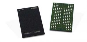
Kioxia Corporation and Western Digital Corp. have developed fifth-gen BiCS flash three-dimensional (3D) flash memory with a 112-layer vertically stacked structure.
Kioxia 5th Gen Bics Flash

Kioxia plans to start shipping samples of this device, which has a 512 gigabit (64GB) capacity with TLC technology, for specific applications in 1FQ20 (1). This device aims to fulfill growing bit demands for a variety of applications, including traditional mobile devices, consumer and enterprise SSDs, emerging applications enabled by the new 5G networks, AI and autonomous vehicles.
Going forward, the firm will apply its fifth-gen process technology to larger capacity devices, such as 1Tb (128GB) TLC and 1.33Tb 4-bit-per-cell (quadruple-level cell, QLC) devices.
The Kioxia’s 112-layer stacking process technology is combined with circuit and manufacturing process technology to increase cell array density by approximately 20% over the 96-layer stacking process. The new technology reduces the cost per bit and increases the manufacturability of memory capacity per silicon wafer. Additionally, it improves interface speed by 50% and offers higher programming performance and shorter read latency.
Since announcing the first (2) prototype 3D flash memory technology in 2007, Kioxia has continued to advance development of 3D flash memory and is actively promoting BiCS flash to meet the demand for larger capacities with smaller die sizes.
5th-gen BiCS flash was developed jointly with technology and manufacturing partner Western Digital Corporation. It will be manufactured at Kioxia’s Yokkaichi Plant and the newly built Kitakami Plant.
Press release from Western Digtital:
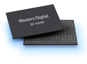
Western Digital Corp. has developed its 5th-gen 3D NAND technology, BiCS5,.
Western Digital Bics5
 BiCS5, built on TLC and QLC technologies, delivers capacity, performance and reliability at a compelling cost. This makes it to address the growth of data associated with connected cars, mobile devices and AI.
The company has commenced initial production of BiCS5 TLC in a 512Gb chip and is currently shipping consumer products built on the new technology. Production of BiCS5 in meaningful commercial volumes is expected in 2Q20. BiCS5 TLC and BiCS5 QLC will be available in a range of capacities, including 1.33Tb. (***)
“As we move into the next decade, a new approach to 3D NAND scaling is critical to continuing to meet the demands of the rising volume and velocity of data,” said Dr. Steve Paak, SVP, memory technology and manufacturing, Western Digital. “Our successful production of BiCS5 is an illustration of Western Digital’s ongoing leadership in flash memory technology and strong execution to our roadmap. By leveraging new advancements to our multi-tier memory hole technology to increase density laterally as well as adding more storage layers, we have scaled the capacity and performance of our 3D NAND technology, while continuing to deliver the reliability and cost which our customers expect.“
Built utilizing a range of new technology and manufacturing innovations, BiCS5 is the company’s highest density and advanced 3D NAND technology to date. Second-gen multi-tier memory hole technology, improved engineering processes and other 3D NAND cell enhancements increase cell array density horizontally across the wafer. These ‘lateral scaling’ advancements in combination with 112 layers of vertical memory capability enables BiCS5 to offer up to 40% (*) more bits of storage capacity per wafer compared to the firm’s 96-layer BiCS4 technology, while optimizing cost. New design enhancements also accelerate performance, enabling BiCS5 to offer up to 50% faster I/O performance compared to BiCS4. (**)
BiCS5 technology was developed jointly with technology and manufacturing partner Kioxia Corporation. It will be manufactured at the joint venture fabrication facilities in Yokkaichi in Mie Prefecture, Japan and Kitakami City, Iwate Prefecture, Japan.
The introduction of BiCS5 technology builds on a portfolio of Western Digital’s 3D NAND technologies for use in data-centric personal electronics, smartphones, IoT devices and data centers.
(1) Not all features have been tested and device characteristics may change in the future.
(2) Source: Kioxia Corporation, as of June 12, 2007.
(*) Based on Western Digital BiCS4 and BiCS5 TLC lowest available and expected-available capacity dies (256Gb and 512Gb die)
(**) Based on Western Digital internal testing of I/O performance in toggle mode for select applications
(***) 1Tb = 1,000,000,000,000 bits
Read also:
Kioxia Devlops Twin BiCS Flash 3D Semicircular Flash Memory Cell Structure
Candidate to surpass QLC for higher memory density and fewer stacking layers
December 16, 2019 | Press Release


 Subscribe to our free daily newsletter


