Arasan: Availability of NAND Flash Controller PHY and I/O Pad IP for 1UMC 28nm SoC Designs Compliant to ONFI 4.1 Specs
NAND flash PHY IP supports 1.2v and 1.8v out of box, 2.5v and 3.3v optionally supported on customer request, ACS ONFI 4.1 PHY IP consisting of 2 major sections DFE and an AFE.
This is a Press Release edited by StorageNewsletter.com on August 30, 2019 at 2:14 pmArasan Chip Systems, Inc. announced the availability of its NAND flash controller PHY and I/O Pad IP for 1UMC 28nm SoC designs compliant to the ONFI 4.1 specs.

The PHY IP is backward compatible with ONFI 4.0 and 3.2 specifications. In addition to the company’s own NAND flash IP controller, the ONFI NAND PHY and I/O Pad IP can also be integrated with customers proprietary NAND flash controllers through a simplified version of the standard DDR DFI Interface. The NAND flash controller IP is a product proven on multiple customer SoC’s and built into some Xilinx FPGA’s.
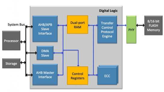
ONFI 4.1 NAND Flash Controller diagram
The company’s NAND flash PHY IP supports 1.2v and 1.8v out of the box. 2.5v and 3.3v are optionally supported on customer request.
ACS ONFI 4.1 PHY IP consists of two major sections DFE and an AFE.
ACS ONFI 4.1 PHY IP DFE contains:
The interface to the NAND flash host controller IP supporting ONFI 4.1 data rates
-
Includes the I/O flops to support both NV_DDR and NV_DDR2, NV_DDR3 operation on the Data Lines.
-
Includes the DLL clocks phase selection logic.
-
Includes data buffering FIFO and ONFI I/O data synchronizing Flops.
-
Includes Scan Logic.
-
Includes BIST to perform self-test and function verification.
ACS ONFI 4.0 PHY AFE contains:
-
ONFI 4.1 IO PADS with integrated ESD protection.
-
CALIO PAD to automatically calibrate the source and sink impedance of ONFI I/O and On Die termination resistors.
-
Retention mode to allow VCORE power down in sleep mode.
-
Analog DLL to provide the following functionality
-
Generates 8 phases equally spaced of TX clock for Tuning to support various hold requirements on the ONFI Data lines at various mode of operation.
-
Generates 8 phases equally spaced of DQS Strobe clock for Tuning function of clocking the incoming data on ONFI IO.
-
DLL clock frequency can be programmed to support any constant clock frequency in the range of 20MHz to 600MHz.
The ONFI 4.1 spec extends NV-DDR3 I/O speeds to 1,066 and 1,200MT/s. For better signaling performance, it adds Duty Cycle Correction (DCC), Read and Write Training for speeds greater than 800MT/s, support for lower pin cap devices with 37.5Ohms default output resistance, and devices which require data burst exit and restart for long data input and output pauses. For lower power, 2.5V Vcc support is added. ONFI 4.1 also includes errata to the ONFI 4.0 spec.
The ONFI 4.1 NAND flash PHY and I/O PAD IP are available for 12nm, 16nm and 28nm SoC designs. Multiple foundries are supported.
Read also:
FMS: Arasan Demos SD Card UHS-II PHY IP and eMMC 5.1 PHY IP for 12nm SoC Designs
And software Stacks and HDK forming Total IP Solution for eMMC and SD Card standards
August 11, 2019 | Press Release


 Subscribe to our free daily newsletter


