Boot ROM and Security for Enterprise SSDs – SK Hynix
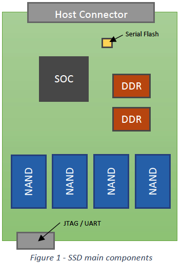
Typical SSD consists of 3 major hardware parts: SOC, DRAM, NAND.
This is a Press Release edited by StorageNewsletter.com on July 17, 2019 at 2:48 pm Typical SSD consists of 3 major hardware parts: SOC, DRAM, NAND, according to Andrei Konan, senior staff firmware engineer, SK Hynix, Inc.
Each of these parts makes a long way to be soldered on the PCB and leave the fab as SSD unit. Behind every major component probably stand months of internal qualifications, years of development, couple of chip re-spins and probably 5 to 10 years of product line evolution and enhancement. Firmware is another key “soft” component of the SSD that is expected to connect all hardware components into the SSD unit, reaching top performance, handling internal errors and complying with customer specifications.
This article intends to cover the means of SSD firmware boot and update as well as related security aspects. In details will discuss about SSD firmware ROM code flow and protection.
Introduction
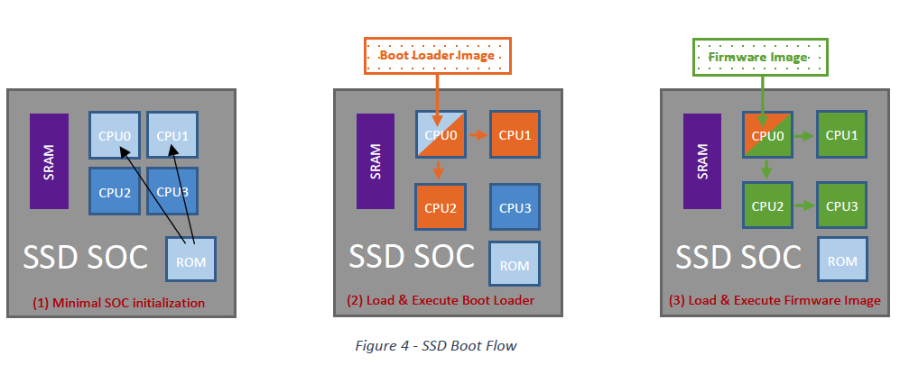
Concept of the ROM code is not new to the SSD industry it is general embedded systems approach to boot the system. At the board power on time ROM code execution is kicked-in as soon as SSD SOC is powered up. Main responsibility of the ROM code is to initialize hardware in very basic manner and load from the non-volatile storage bootloader mini image with reach functionality that particularly can load and boot firmware image.

ROM Hardware Initialization
Hardware initialization in ROM code is mainly related to the SOC configuration in order to bring-up basic NAND operations and host protocol (SATA, PCIe) enable. ROM code is usually very simple and straightforward. Keeping it simple helps to minimize SOC re-spins due to ROM bugs.
For example, DRAM is typically not initialized by ROM code as DRAM PHY settings are quite complicated and requires regular tuning depending on the multiple factors like PCB signal integrity, maturity of DRAM technology itself, migration to the new DRAM chips, etc. Another good example for the ROM simplicity is the requirement to support various NAND technologies (like MLC, TLC, QLC and couple of different layered technologies). It means for the bootloader image read from NAND – the simplest way should be chosen, that is supported by major NAND technologies. Host protocol initialization is usually required for manufacturing process to load initial firmware to the fresh drive.

ROM Fresh Drive Firmware Update
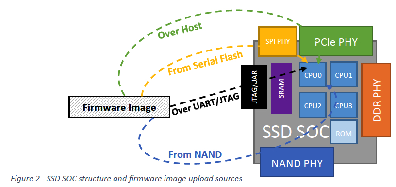
Typically, firmware update for the fresh SSD is done using UART, host or even JTAG interface in order to transfer firmware image to the SOC internal memory and flush to the NAND, so after power cycle the drive can boot up successfully for the first time. It is vital to support multiple ways for the fresh firmware download, first for the backup reasons, second for convenience, third for equipment reasons. Local SSD engineers may prefer JTAG method for the speed reasons and convenience. Manufacturing department most likely will use host interface. Testing teams prefer UART.
ROM Code and Serial flash
It sounds weird that enterprise SSD may require EEPROM (serial flash) to boot. For sure it is not for mass production but for debug reasons mainly during product development. Imagine situation that SSD company is developing new SOC generation. It will require new ROM code.
Before actual silicon will leave the fab – the only ways to verify ROM code functionality is either using FPGA or Simulation. Both do not guarantee 100% ROM operation within a final top speed silicon. In case ROM code is not working after first SOC tape out – it is possible to force SSD to boot from serial flash. It can be programmed with the patched (fixed) version of the ROM code. In this case native ROM code is just reading image in serial flash chip and jumps into it. Lack of security protection for the engineering methods to boot the SSD may lead to the Security issues like CVE-2019-10636 exposed recently in Marvell SSD controllers.
Firmware Image Binary
SSD firmware Image consists usually of 3 major parts: (a) header, (b) image directory, (c) footer. There is no SSD industry standard related to the firmware image format thus it is fully vendor specific. Technically there is nothing SSD special in mentioned generic layout of firmware image. Probably the only specifics may be found in item (b) image directory. Customers and users prefer single image binary that can be loaded to the drives of all capacities. In order to comply with this – SSD vendors typically glue binaries of all capacities into the directory and SDD by itself upon image receive decides what binary from the directory to load and apply. Header is vendor specific descriptor of the image. Footer has RSA signature that covers both Header and the image directory.

Field Firmware Image Update
As soon as SSD unit is leaving factory, there is only one way to update the firmware – using host protocol (SATA, SAS, NVMe) command. As time goes SSD vendor can distribute firmware images with stability fixes. Basically, it is signed binary image of the structure mentioned above. Upon new firmware image receipt – SSD verifies digital signature and stores new image to the NAND in addition to already existing images or replacing them. Secure update process requires entire binary storage (with header and footer) to NAND as each power up – Boot ROM will need to verify the image read from NAND. In addition, update procedure may require bootloader code extraction from the main firmware Image and storing it in separate location again in a secure manner using digital signature. It is very critical to store firmware image in NAND in very secured manner. Secured in terms of storage endurance. To reach this SSD vendors are using mirroring of the image in different NAND chips plus using special firmware SLC NAND mode that guarantees typically 5 years retention without the need for data refresh.

ROM Code Boot Flow
ROM code reads bootloader from the NAND and boots into it. Bootloader is in charge to read firmware image and reboot into it. Nowadays SSD SOCs are built with multiples CPUs inside for various purposes (host protocol core, mapping core, NAND sequencer core, etc.) In order to minimize complexity of ROM code – it usually initializes minimal number of CPUs within SOC needed for the basic NAND operations. Bootloader in its turn after loading main firmware image must load all CPUs with code plus load external to CPUs memories (SRAM, DRAM) with code and data as well. In the end bootloader is releasing all CPUs for execution and SSD firmware code starts running.
Firmware Image Security
Key point for the image security is inability to load custom or cracked images via all available interfaces (host protocol, UART, JTAG, serial flash). The only one safe method to be left is protocol (NVMe, SATA, SAS) firmware image update with the binary signed by the vendor. Drive security requires all debug features (UART, JTAG, serial flash) disable once SSD leaves the fab. Even with physical access to the drive hacker should not be able to use debug backdoors to access and change the firmware image. Mentioned requirements are satisfied usually by burning SOC FUSE bits related to the physical disable of debug features without an ability to change the drive state back to debug one.
SSD vendors ship the same firmware image to different customers. Each customer usually requires firmware image to be signed by unique RSA keys. Sometimes even customers are doing firmware signing by themselves. In order to accommodate the requirements, it is usually required for SSD vendors to have protection for both firmware image and customer id. SK Hynix was granted recently with patent to protect SSD firmware binaries. Key point is to introduce customer specific protected area in firmware image to accommodate the requirements. It allows enterprise SSDs to operate safely in storage centers and pr otect user information from being hacked and stolen.
Read also:
Patent: Semiconductor memory system and operating method thereof


 Subscribe to our free daily newsletter


