Renesas Develops Flash Memory With OTA Support in Automotive Microcontrollers Based on 28nm Process
Achieves 24MB capacity of embedded flash memory and 240MHz random access operation.
This is a Press Release edited by StorageNewsletter.com on June 21, 2019 at 2:09 pmRenesas Electronics Corporation announced the development of a flash memory technology that achieves larger memory capacities, higher readout speeds, and over-the-air (OTA) support for automotive microcontrollers (MCUs) using the next-gen 28nm process.
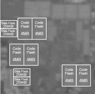
This technology achieves an industry’s large capacity of embedded flash memory on an MCU – 24MB – and reaches 240MHz random access read speeds, an industry’s fast for embedded flash memory.
The technology also achieves low noise write operations when performing OTA wireless software updates, and high-speed and robust operation for OTA software updates.
The company presented these results on June 12 at the 2019 Symposia on VLSI Technology and Circuits in Kyoto, Japan, June 9-14, 2019.
Recently in technologies used in car systems, such as autonomous driving and electric drive, there have been increasing demands for larger embedded flash memory capacities in the MCUs due to the increasing scale of the control software.
The introduction of OTA technology accelerates the demand for larger capacities to assure adequate storage area for updated programs. Since it is necessary to assure real-time performance given the addition of new functions such as functional safety, faster random access read times from the flash memory are also desired.
Furthermore, regarding OTA, 3 things are strongly desired. First is low-noise design so that the updated software can be stored reliably even when the car is operating. Second is reduced down time during the software switching. Third is robustness to avoid incorrect operations even if unintentional interruptions occur when updating or switching software.
Developed flash memory technology addresses demands with:
-
24MB on-chip flash memory – industry’s large in MCU
Renesas continues to adopt the high-speed, high-reliability SG-MONOS (1) technology for the embedded flash memory used in its MCUs. The memory cell size of the 28nm generation developed here is reduced by more than 15%, from the earlier 0.053µm to smaller than 0.045µm. While suppressing increases in the chip size, this technology allows the inclusion of 24MB of code storage flash memory, the industry’s largest capacity for embedded flash memory. The company has also included 1MB of storage flash memory in the test chip for parameters and other data. -
240MHz random access read speed – an industry’s high speeds for MCUs with embedded flash memory
Word line division is an effective method for increasing the speed of random access reads in embedded flash memory. However, this division increases the number of word line drivers and causes reliability degradation due to time-dependent dielectric breakdown (TDDB) of the transistors included in those drivers and word line supply voltage drops due to increased leakage current. Renesas resolved these issues using word line driver stress mitigation and distributed word line supply voltage drivers and has verified 240MHz speed random access, the industry’s highest in a test chip, over junction temperatures from -40°C to 170°C.
Development of noise-reducing technology
By changing the write current applied to each memory cell between initial operation and later operation when programming the flash memory, the firm has reduced the peak current consumption from the external power supply (Vcc) by 55% without reducing the throughput compared to earlier Renesas devices. This suppresses the adverse influence of supply voltage noise on the MCU itself during OTA operations when the car is running. The company has also applied the idea of varying the write current to high-speed write mode, in which the number of simultaneously programmed cells is increased. As a result, this device achieves speed programming at 6.5MB/s in this mode. This makes it possible to suppress the increased test times associated with the large memory capacity.
OTA capable of control software switching that is robust and fast
In this test chip, the code storage flash memory is divided into a storage area for software in use and a storage area for updated software. This makes it possible to switch the software in less than one milliseconds at ignition off. Furthermore, the software switching settings are duplicated and new state flags were added to prevent incorrect operation in the event that the software updates or switching is unintentionally interrupted. This achieves, at the same time, the operation that allows executable control software to be selected reliably and a reduction of down time during which the car cannot be used.
The above technologies make it possible to support the increasing scales of automotive control software, high-speed real-time control, and OTA. Moving forward, the firm is committed to continued development of embedded flash memory and striving to achieve the higher capacities, higher speeds, and lower power consumption that will be required to support new applications.
(1) MONOS: Metal-oxide-nitride-oxide-silicon. A technology that Renesas has achieved a substantial track record of over 20 years in EEPROM, secure MCU, and other products. The technology is used in the embedded flash memory used in Renesas MCUs.
(2) A Renesas flash memory technology announced at the 2015 International Solid-State Circuits Conference (ISSCC 2015).


 Subscribe to our free daily newsletter

