


R&D: Optical Memory Cell Achieves Record Storage Density
Device could enable computers that use optics and electrical signals to interact with data.
This is a Press Release edited by StorageNewsletter.com on December 26, 2018 at 2:14 pmResearchers have demonstrated a technique that can store more optical data in a smaller space than was previously possible on-chip.
Technique allows more optical data to be stored in smaller space
than was previously possible on-chip.
This demonstration is important step toward all-optical computer.
(Credit: Oxford University)

This technique improves upon the phase-change optical memory cell, which uses light to write and read data, and could offer a faster, more power-efficient form of memory for computers.
In Optica, The Optical Society (OSA)’s journal for high impact research, researchers from the Universities of Oxford, Exeter and Münster describe their technique for all-optical data storage, which could help meet the growing need for more computer data storage.
Rather than using electrical signals to store data in one of two states – a zero or one – like today’s computers, the optical memory cell uses light to store information. The researchers demonstrated optical memory with more than 32 states, or levels, the equivalent of five bits. This is an important step toward an all-optical computer, a long-term goal of many research groups in this field.
“Optical fibers bring light-encoded data to our homes and offices, but that information is transformed to electronic signals once inside computers,” said Harish Bhaskaran, leader, research team, Oxford University. “By bringing the speed of light-based data transmission to the circuit boards that run computers, our all-optical memory could enable a hybrid computer chip that interacts with data both optically and electrically.”
This work is part of a large project called Fun-COMP (Functionally-scaled Computing technology), that brings academic and industrial partners together to develop groundbreaking hardware technologies.
 (Credit: Oxford University)
Writing data with light
The optical memory cell uses light to encode information in a phase change material, a class of materials used to make re-writable CDs and DVDs. A laser heats portions of a phase change material, which causes it to switch between states where all the atoms are ordered or disordered. Because these two states exhibit different optical indices of refraction, the data can be read using light.
Phase change materials can store data for a long time because they remain in the disordered or ordered state until illuminated again with the specific type of laser light originally used to write the data. Mixing different ratios of ordered and disordered states in an area of the material allows information to be stored in a continuum of levels instead of just a zero and a one as in traditional electronic memory.
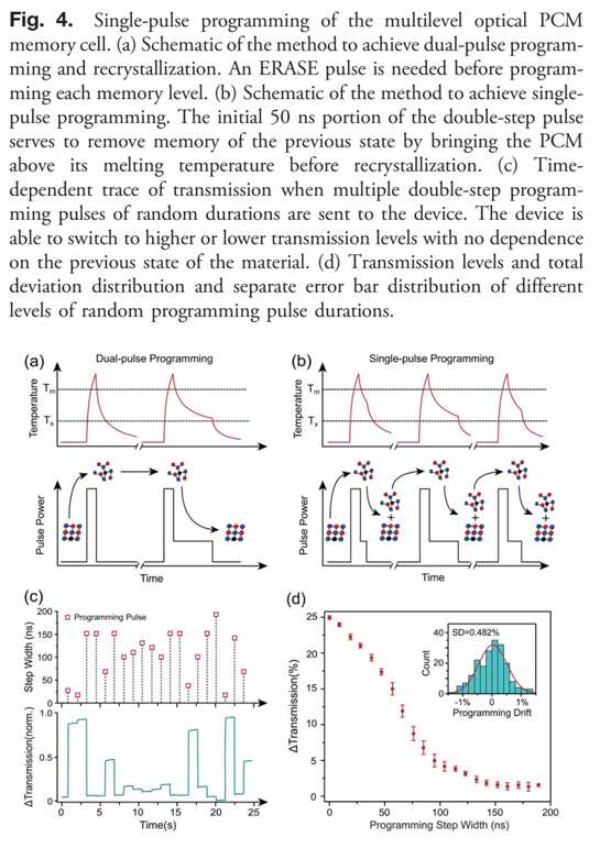
“Although our team has previously used this approach to optical memory, we’ve now been able to push the resolution limits of this memory cell by storing a larger number of intermediate states between zero and one,” said Nathan Youngblood, member, research team. “This allowed us to store information in 34 levels, while only ten could be achieved previously.”
The researchers accomplished the increased resolution by using a new technique they developed that uses laser light with a single, double-stepped pulse – two pulses put together into a rectangular-shaped pulse – to precisely control the melting and the crystallization of the material.
“Instead of heating the material with a single laser pulse, we shape the pulse in a way that allows us to control the material’s temperature over time,” said Xuan Li, paper’s first author. “This provides the ability to adjust how that material interacts with light and the state it will reach after heating. It also greatly speeds up the writing process because we can change the material’s state with just one laser pulse instead of the hundreds or thousands of pulses required previously.”
Multi-level memory storage
In the paper, the researchers showed that they could use their approach to reliably encode data on 34 levels, which is more than the 32 levels necessary to achieve five-bit programming.
“This accomplishment required understanding the interaction between the light and the material perfectly and then sending exactly the right sort of laser pulse necessary to achieve each level,” said Bhaskaran. “We solved an extraordinarily difficult problem.”
This technique could help overcome one of the bottlenecks limiting the speed of today’s computers: the link between the processor and the memory.
“A lot of work has gone into improving the communication between these two units using fiber optics,” said Bhaskaran. “However, linking these two units optically still requires expensive electro-optical conversions at both ends. Our memory cell could be used in a hybrid optical-electrical setup to eliminate the need for that conversion on the memory side by allowing data to be stored and retrieved optically.”
Next the researchers want to integrate multiple memory cells and individually program them, which would be required to make a working memory chip for a computer. The research groups have been working closely with Oxford University Innovation, the University’s Innovation arm, to develop commercial opportunities arising from their research on photonic memory cells. The researchers say that they can already replicate the devices extremely well but will need to develop light signal processing techniques to integrate multiple optical memory cells.
Paper: Fast and reliable storage using a five-bit, non-volatile photonic memory cell
Optica has published an article written by Xuan Li, Nathan Youngblood, Department of Materials, University of Oxford, Oxford, UK , Carlos Ríos,Department of Materials, University of Oxford, Oxford, UK, and Department of Materials Science & Engineering, Massachusetts Institute of Technology, Cambridge, Massachusetts 02139, USA, Zengguang Cheng,Department of Materials, University of Oxford, Oxford, UK, C. David Wright,Department of Engineering, University of Exeter, Exeter, UK, Wolfram HP Pernice,Department of Physics, University of Münster, Münster, Germany , and Harish Bhaskaran, Department of Materials, University of Oxford, Oxford, UK.
Click to enlarge
Abstract : “Optically storing and addressing data on photonic chips is of particular interest as such capability would eliminate optoelectronic conversion losses in data centers. It would also enable on-chip non-von Neumann photonic computing by allowing multinary data storage with high fidelity. Here, we demonstrate such an optically addressed, multilevel memory capable of storing up to 34 nonvolatile reliable and repeatable levels (over five bits) using the phase change material Ge2Sb2Te5 integrated on a photonic waveguide. Crucially, we demonstrate for the first time, to the best of our knowledge, a technique that allows us to program the device with a single pulse regardless of the previous state of the material, providing an order of magnitude improvement over previous demonstrations in terms of both time and energy consumption. We also investigate the influence of write-and-erase pulse parameters on the single-pulse recrystallization, amorphization, and readout error in our multilevel memory, thus tailoring pulse properties for optimum performance. Our work represents a significant step in the development of photonic memories and their potential for novel integrated photonic applications.“
About Optica
Optica is an open-access, online-only journal dedicated to the rapid dissemination of high-impact peer-reviewed research across the entire spectrum of optics and photonics. Published monthly by The Optical Society (OSA), Optica provides a forum for pioneering research to be swiftly accessed by the international community, whether that research is theoretical or experimental, fundamental or applied. Optica maintains a distinguished editorial board of more than 50 associate editors from around the world and is overseen by Alex Gaeta, editor-in-chief, Columbia University, USA.
About Optical Society
Founded in 1916, The Optical Society (OSA) is a professional organization for scientists, engineers, students and business leaders who fuel discoveries, shape real-life applications and accelerate achievements in the science of light. Through world-renowned publications, meetings and membership initiatives, OSA provides quality research, inspired interactions and dedicated resources for its extensive global network of optics and photonics experts.


 Subscribe to our free daily newsletter

