


R&D: Scientists Technique to Boost Capacity of Computer Storage Thousandfold
Technique leads to world’s densest solid-state memory that can store 45 million songs on surface of quarter.
This is a Press Release edited by StorageNewsletter.com on July 30, 2018 at 2:26 pmBy Jennifer-Anne Pascoe, University of Alberta
The most dense solid-state memory ever created could soon exceed the capabilities of current computer storage devices by 1,000 times, thanks to a new technique scientists at the University of Alberta have perfected.
Roshan Achal (left) used nanotechnology perfected by his PhD supervisor, Robert Wolkow (right) to create atomic-scale computer memory that could exceed the capacity of today’s solid-state storage drives by 1,000 times.
(Photo: Faculty of Science)

“Essentially, you can take all 45 million songs on iTunes and store them on the surface of one quarter,” said Roshan Achal, PhD student,department of physics and lead author on the new research. “Five years ago, this wasn’t even something we thought possible.”
The scientists used the same technology they developed to manufacture atomic-scale circuits, which allows for quickly removing or replacing single hydrogen atoms. The technology enables the memory to be rewritable, meaning it could lead to far more efficient types of solid-state drives for computers.
“What is often overlooked in the nanofabrication business is actual transportation to an end-user, which simply was not possible until now given temperature restrictions,” noted Achal. “Our memory is stable well above room temperature and precise down to the atom.”
Achal explained the technology has immediate applications for archiving data. Next steps will include increasing read and write speeds for even more flexible applications.
More memory, less space
Achal works with U of A physics professor Robert Wolkow, a pioneer in the field of atomic-scale physics. Wolkow perfected the nanotip technology that allows scientists to manipulate single atoms on a silicon chip—a technology he said has now reached a tipping point.
“With this last piece of the puzzle now in hand, atom-scale fabrication will become a commercial reality in the very near future,” said Wolkow. His spinoff company, Quantum Silicon Inc., is working on commercializing atom-scale fabrication for use in all areas of the technology sector.
To demonstrate the new memory, Achal, Wolkow and their fellow scientists encoded the entire alphabet at a density of 138TB per square inch, roughly equivalent to writing 350,000 letters across a grain of rice. For a playful twist, Achal also encoded music reminiscent of video game soundtracks from the ‘80s and ‘90s.
The research, Lithography for Robust and Editable Atomic-Scale Silicon Devices and Memories, appears in the current issue of Nature Communications.
Resources:
Related: Atomic-scale manufacturing sets forth electronics revolution akin to arrival of printing press
Related: Atomic discovery opens door to greener, faster, smaller electronic circuitry
Video: Music stored in smallest stable rewritable atomic memory
Article: Lithography for robust and editable atomic-scale silicon devices and memories
Nature Communications has published an article written by Roshan Achal, Mohammad Rashidi, Department of Physics, University of Alberta, Edmonton, AB, T6G 2E1, Canada, and Quantum Silicon, Inc., Edmonton, AB, T6G 2M9, Canada, Jeremiah Croshaw, Department of Physics, University of Alberta, Edmonton, AB, T6G 2E1, Canada, David Churchill, Memorial University of Newfoundland, St. John’s, NL, A1B 3X5, Canada, Marco Taucer, Taleana Huff, Department of Physics, University of Alberta, Edmonton, AB, T6G 2E1, Canada, and Quantum Silicon, Inc., Edmonton, AB, T6G 2M9, Canada, Martin Cloutier, Nanotechnology Research Centre, National Research Council of Canada, Edmonton, AB, T6G 2M9, Canada, Jason Pitters, Quantum Silicon, Inc., Edmonton, AB, T6G 2M9, Canada, and Nanotechnology Research Centre, National Research Council of Canada, Edmonton, AB, T6G 2M9, Canada, and Robert A. Wolkow, Department of Physics, University of Alberta, Edmonton, AB, T6G 2E1, Canada, Quantum Silicon, Inc., Edmonton, AB, T6G 2M9, Canada, and Nanotechnology Research Centre, National Research Council of Canada, Edmonton, AB, T6G 2M9, Canada.
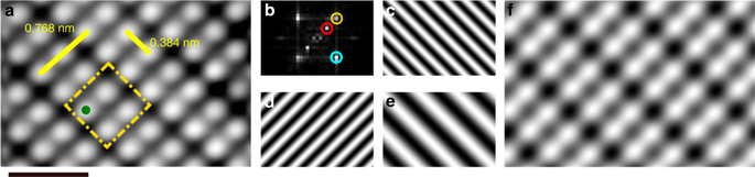
Surface geometry of hydrogen-passivated Si(100)-2×1. a (V = 1.4 V, I = 50 pA, T = 4.5 K, 2 × 3 nm2) Scanning tunneling microscope (STM) image of hydrogen atoms bonded to the Si(100)-2×1 surface. The distance between identical sites along and across a dimer row are shown in yellow (solid). The surface geometry allows for the creation of single atom bits at ultra-high densities. The area of one bit (including spaces between atoms), 0.590 nm2, is outlined in yellow (dashed), and is defined as a binary zero. The hydrogen atom denoted with a dot (green) is removed with an STM tip to create a dangling bond, changing the bit to a binary one. b 2D-Fourier transform (power spectrum) of a, where the three dominant spatial frequencies have been isolated. c–e Filtered STM images of a, for each dominant frequency (peak) shown in b, c bottom peak (blue), d top peak (yellow), e middle peak (red). f The resulting image from the sum of frequencies shown in c–e, reconstructing the essential features of the STM image shown in a, allowing for the position of each surface hydrogen atom to be determined. Scale bar, 1 nm.
Abstract: “At the atomic scale, there has always been a trade-off between the ease of fabrication of structures and their thermal stability. Complex structures that are created effortlessly often disorder above cryogenic conditions. Conversely, systems with high thermal stability do not generally permit the same degree of complex manipulations. Here, we report scanning tunneling microscope (STM) techniques to substantially improve automated hydrogen lithography (HL) on silicon, and to transform state-of-the-art hydrogen repassivation into an efficient, accessible error correction/editing tool relative to existing chemical and mechanical methods. These techniques are readily adapted to many STMs, together enabling fabrication of error-free, room-temperature stable structures of unprecedented size. We created two rewriteable atomic memories (1.1 petabits per in2), storing the alphabet letter-by-letter in 8 bits and a piece of music in 192 bits. With HL no longer faced with this trade-off, practical silicon-based atomic-scale devices are poised to make rapid advances towards their full potential.“


 Subscribe to our free daily newsletter

