R&D: Using Light for Next Gen Storage
Platform has potential to be extended to 2D and 3D memory for densities that could potentially approach petabyte/cm3 levels.
This is a Press Release edited by StorageNewsletter.com on July 5, 2018 at 2:10 pmFrom University of South Australia
Tiny, nano-sized crystals of salt encoded with data using light from a laser could be the next data storage technology of choice, following research by Australian scientists.
Scientists Xuanzhao Pan and Dr Nick Riesen
demonstrating novel optical data storage platform
(Credit: Elizaveta Klantsataya)
The researchers from the University of South Australia and University of Adelaide, in collaboration with the University of New South Wales, have demonstrated a novel and energy-efficient approach to storing data using light.
“With the use of data in society increasing dramatically due to the likes of social media, cloud computing and increased smart phone adoption, existing data storage technologies such as hard drive disks and solid-state storage are fast approaching their limits,” says project leader Dr Nick Riesen, research fellow, University of South Australia. “We have entered an age where new technologies are required to meet the demands of 100s of terabyte (1000 gigabytes) or even petabyte (one million gigabytes) storage. One of the most promising techniques of achieving this is optical data storage.”
Dr Riesen and Xuanzhao Pan, PhD student, University of Adelaide, developed technology based on nanocrystals with light-emitting properties that can be efficiently switched on and off in patterns that represent digital information. The researchers used lasers to alter the electronic states, and therefore the fluorescence properties, of the crystals.
Their research shows that these fluorescent nanocrystals could represent a promising alternative to traditional magnetic HDD and SSD storage or blu-ray discs. They demonstrated rewritable data storage in crystals that are 100s of times smaller than that visible with the human eye.
“What makes this technique for storing information using light interesting is that several bits can be stored simultaneously. And, unlike most other optical data storage techniques, the data is rewritable,” says Dr Riesen.
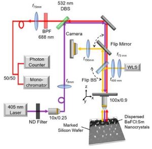
Fig. 1 Experimental setup with custom scanning confocal microscope arrangement for read-out.
Solid lines represent fibers, glowing lines are free-space propagation.
BPF: Bandpass filter,
BS: Beamsplitter,
DBS: Dichroic beamsplitter, ++
WLS: White light source.
(© 2018 Optical Society of America)
Click to enlarge
This ‘multilevel data storage’ – storing several bits on a single crystal – opens the way for much higher storage densities. The technology also allows for very low-power lasers to be used, increasing its energy efficiency and being more practical for consumer applications.
“The low energy requirement also makes this system ideal for optical data storage on integrated electronic circuits,” says Professor Hans Riesen, University of New South Wales.
“These results showcase the benefits of establishing complementary research capabilities and infrastructure at collaborating universities – this has been a deliberate strategy in the photonics domain that is bearing fruit across a number of projects,” says Professor Tanya Monro, DVC-R, University of South Australia.
The technology also has the potential to push forward the boundaries of how much digital data can be stored through the development of 3D storage.
“We think it’s possible to extend this data storage platform to 3D technologies in which the nanocrystals would be embedded into a glass or polymer, making use of the glass-processing capabilities we have at IPAS,” says Professor Heike Ebendorff-Heidepriem, University of Adelaide. “This project shows the far-reaching applications that can be achieved through transdisciplinary research into new materials.”
Dr Riesen says: “3D optical data storage could potentially allow for up to petabyte level data storage in small data cubes. To put that in perspective, it is believed that the human brain can store about 2.5 petabytes. This new technology could be a viable solution to the great challenge of overcoming the bottleneck in data storage.”
Article: Towards rewritable multilevel optical data storage in single nanocrystals
Optics Express has published an article written by Nicolas Riesen, University of South Australia and Future Industries Institute, Mawson Lakes, SA 5095, Australia, and Institute for Photonics and Advanced Sensing (IPAS) and School of Physical Sciences, The University of Adelaide, SA 5005, Australia, Xuanzhao Pan, Institute for Photonics and Advanced Sensing (IPAS) and School of Physical Sciences, The University of Adelaide, SA 5005, Australi, Kate Badek, School of Physical, Environmental and Mathematical Sciences, The University of New South Wales, Canberra, ACT 2600, Australia, Yinlan Ruan, Institute for Photonics and Advanced Sensing (IPAS) and School of Physical Sciences, The University of Adelaide, SA 5005, Australia, Tanya M. Monro, University of South Australia and Future Industries Institute, Mawson Lakes, SA 5095, Australia, and Institute for Photonics and Advanced Sensing (IPAS) and School of Physical Sciences, The University of Adelaide, SA 5005, Australia, Jiangbo Zhao, Heike Ebendorff-Heidepriem, Institute for Photonics and Advanced Sensing (IPAS) and School of Physical Sciences, The University of Adelaide, SA 5005, Australia, and Hans Riesen, School of Physical, Environmental and Mathematical Sciences, The University of New South Wales, Canberra, ACT 2600, Australia.
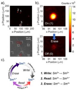
Fig. 3 Nanocrystal bleaching/erasure demonstration. (a) SCM image of BaFCl:Sm3+ nanoaggregates of 2-3 crystals C1, C2 and C3 after exposure to UV-C (λ ~185 nm, t >10 mins, P~200 µW/cm2) and corresponding SEM (ETD) image. (b) Subsequent On-Off state erasure (λ = 405 nm, P = 220 µW) of C3 (with read-out λex = 405 nm, P = 50 µW, λem = 687.8 nm, 5D0→7F0). (c). Schematic of write-read-erase mechanism for BaFCl:Sm.
(© 2018 Optical Society of America)
Click to enlarge
Abstract: “Novel approaches for digital data storage are imperative, as storage capacities are drastically being outpaced by the exponential growth in data generation. Optical data storage represents the most promising alternative to traditional magnetic and solid-state data storage. In this paper, a novel and energy efficient approach to optical data storage using rare-earth ion doped inorganic insulators is demonstrated. In particular, the nanocrystalline alkaline earth halide BaFCl:Sm is shown to provide great potential for multilevel optical data storage. Proof-of-concept demonstrations reveal for the first time that these phosphors could be used for rewritable, multilevel optical data storage on the physical dimensions of a single nanocrystal. Multilevel information storage is based on the very efficient and reversible conversion of Sm3+ to Sm2+ ions upon exposure to UV-C light. The stored information is then read-out using confocal optics by employing the photoluminescence of the Sm2+ ions in the nanocrystals, with the signal strength depending on the UV-C fluence used during the write step. The latter serves as the mechanism for multilevel data storage in the individual nanocrystals, as demonstrated in this paper. This data storage platform has the potential to be extended to 2D and 3D memory for storage densities that could potentially approach petabyte/cm3 levels.”
© 2018 Optical Society of America under the terms of the OSA Open Access Publishing


 Subscribe to our free daily newsletter

