


Qualification of Embedded SuperFlash Technology on 40nm CMOS Process for SST
More than 20% reduction in embedded flash cell size, and 20 to 30% reduction in macro area over 55nm process
This is a Press Release edited by StorageNewsletter.com on May 11, 2018 at 2:32 pmThe amount of data processed in IoT applications continues to increase, making low power and high density paramount to system designers.
Many IC designers are turning to single-chip solutions to implement these features, saving total system costs by combining digital, analog, RF, microcontroller (MCU) and embedded flash memory on a monolithic device.
To meet these needs, Microchip Technology Inc. subsidiary Silicon Storage Technology, Inc. (SST), and United Microelectronics Corporation, a global semiconductor foundry, announced the full qualification and availability of SST’s embedded SuperFlash non-volatile memory on UMC’s 40nm CMOS platform. The 40nm process features a more than 20% reduction in embedded flash cell size and a 20-to-30% reduction in macro area over their 55nm process.
The endurance of embedded SuperFlash IP offers SoC customers reliability and design flexibility combined with reduced power usage. This non-volatile memory technology is qualified for a minimum of 100,000 cycles, underscoring the technology’s reliability. For edge computing in IoT devices, SuperFlash technology features power benefits that derive from low-power standby and read operations, with core supply at 0.81V. It also secures applications with code maintained on chip, which is the first step in preventing illegal access through hardware and software attacks.
“The 40nm qualification represents another milestone in our partnership with MC,” said Vipin Tiwari, director, WW business development and marketing, SST. “SuperFlash technology continues to be the most reliable embedded flash memory in the semiconductor industry, providing customers across broad markets the low-power, high-density features their products depend on.”
“With the positive response and success from customers who used SST’s 55nm SuperFlash technology, we are pleased to offer our customers another process platform with characteristics that fit a range of IoT applications,” said Wenchi Ting, associate VP, specialty technology division, UMC. “The addition of the fully qualified 40 nm SST SuperFlash will further enrich our IP portfolio of high-quality embedded memory solutions.“
The SuperFlash technology complements UMC’s embedded memory portfolio with high density and low-power IP. Combined with the company’s inherent technology reliability, the firm’s flexible capacity and high-yield maturity for its 55nm and 40nm platform provide foundry customers the manufacturing support needed to build a range of product applications.
To date, more than 80 billion units have shipped with the embedded SuperFlash technology.
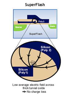
It is based on a proprietary split-gate flash memory cell with the following capabilities:
-
Low-power program, erase and read operations
-
Performance with fast read access
-
Scalability from 1µm technology node to 28nm technology node
-
High endurance cycling up to 500,000 cycles
-
Data retention of over 20 years
-
Performance at high temperature for automotive-grade applications
-
Immunity to Stress-Induced Leakage Current (SILC)


 Subscribe to our free daily newsletter

