


R&D: Ultra-Thin Memory Storage Device Paves Way for More Powerful Computing
Alternative ways to provide greater memory storage capacity on even smaller computer chips
This is a Press Release edited by StorageNewsletter.com on January 22, 2018 at 2:15 pmSource: The University of Texas At Austin
Engineers worldwide have been developing alternative ways to provide greater memory storage capacity on even smaller computer chips. Previous research into two-dimensional atomic sheets for memory storage has failed to uncover their potential – until now.
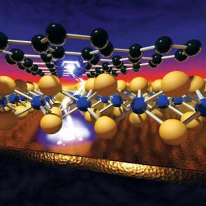
Illustration of a voltage-induced memory effect in monolayer nanomaterials,
which layer to create ‘atomristors,’ the thinnest memory storage device
that could lead to faster, smaller and smarter computer chips.
(Cockrell School of Engineering)
A team of electrical engineers at The University of Texas at Austin, in collaboration with Peking University scientists, has developed the thinnest memory storage device with dense memory capacity, paving the way for faster, smaller and smarter computer chips for everything from consumer electronics to big data to brain-inspired computing.
“For a long time, the consensus was that it wasn’t possible to make memory devices from materials that were only one atomic layer thick,” said Deji Akinwande, associate professor, department of electrical and computer engineering, Cockrell School of Engineering. “With our new ‘atomristors,’ we have shown it is indeed possible.”
Made from 2-D nanomaterials, the ‘atomristors’ – a term Akinwande coined – improve upon memristors, an emerging memory storage technology with lower memory scalability. He and his team published their findings in the January issue of Nano Letters.
“Atomristors will allow for the advancement of Moore’s Law at the system level by enabling the 3-D integration of nanoscale memory with nanoscale transistors on the same chip for advanced computing systems,” Akinwande said.
Memory storage and transistors have, to date, always been separate components on a microchip, but atomristors combine both functions on a single, more efficient computer system. By using metallic atomic sheets (graphene) as electrodes and semiconducting atomic sheets (molybdenum sulfide) as the active layer, the entire memory cell is a sandwich about 1.5 nanometers thick, which makes it possible to densely pack atomristors layer by layer in a plane. This is a substantial advantage over conventional flash memory, which occupies far larger space. In addition, the thinness allows for faster and more efficient electric current flow.
Given their size, capacity and integration flexibility, atomristors can be packed together to make advanced 3-D chips that are crucial to the successful development of brain-inspired computing. One of the greatest challenges in this burgeoning field of engineering is how to make a memory architecture with 3-D connections akin to those found in the human brain.
“The sheer density of memory storage that can be made possible by layering these synthetic atomic sheets onto each other, coupled with integrated transistor design, means we can potentially make computers that learn and remember the same way our brains do,” Akinwande said.
The research team also discovered another unique application for the technology. In existing ubiquitous devices such as smartphones and tablets, radio frequency switches are used to connect incoming signals from the antenna to one of the many wireless communication bands in order for different parts of a device to communicate and cooperate with one another. This activity can significantly affect a smartphone’s battery life.
The atomristors are the smallest radio frequency memory switches to be demonstrated with no DC battery consumption, which can ultimately lead to longer battery life.
“Overall, we feel that this discovery has real commercialization value as it won’t disrupt existing technologies,” Akinwande said. “Rather, it has been designed to complement and integrate with the silicon chips already in use in modern tech devices.”
Funding for the UT Austin team’s work was provided by the National Science Foundation and the Presidential Early Career Award for Scientists and Engineers, which Akinwande was awarded in 2015.
Article: Atomristor: Nonvolatile Resistance Switching in Atomic Sheets of Transition Metal Dichalcogenides
Nano Letters has published an article written by Ruijing Ge, Xiaohan Wu, Myungsoo Kim, Microelectronics Research Center, The University of Texas at Austin, Austin, Texas 78758, United States,Jianping Shi, Department of Materials Science and Engineering, College of Engineering, Peking University, Beijing 100871, China, Sushant Sonde, Institute for Molecular Engineering, University of Chicago, 5640 South Ellis Avenue, Chicago, Illinois 60637, United States, and Center for Nanoscale Materials, Argonne National Laboratory, 9700 Cass Avenue, Lemont, Illinois 60439, United States, Li Tao, School of Materials Science and Engineering, Southeast University, 2 Southeast University Road, Nanjing 211189, China, and Microelectronics Research Center, The University of Texas at Austin, Austin, Texas 78758, United States, Yanfeng Zhang, Department of Materials Science and Engineering, College of Engineering, Peking University, Beijing 100871, China, Jack C. Lee, and Deji Akinwande, Microelectronics Research Center, The University of Texas at Austin, Austin, Texas 78758, United States.
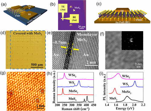
Figure 1. Schematic, device, and material characterization. (a, b)
Schematic and optical image of metal–insulator–metal structures of TMD
crossbar sandwich. (c) Schematic of TMD lithography-free and transfer-free sandwich
(TE and BE are gold, if not specified) based on MoS2 grown on Au foil. (d)
Optical image of fabricated MoS2 litho-free devices with Au electrodes on Si/SiO2
substrate. The dash box in panel d indicates the area covered with MoS2. (e)
TEM cross-section image of Au/MoS2/Au litho-free device revealing the atomically sharp
and clean monolayer interface. (f) Atomic resolution TEM image of MoS2 after
transfer onto TEM grid. The hexagonal honeycomb structure has an in-plane lattice constant ∼0.31 nm
indicating high-quality synthesized MoS2.
Inset: selective area electron diffraction (SAED) pattern captured from MoS2
film, consisting of only one set of hexagonally arranged diffraction spots,
suggestive of single-crystal growth. (g) Atomically resolved STM images
of monolayer MoS2 on Au(100). The S vacancy defects (∼1012/cm2) are indicated
by the dashed circle. (h, i) Raman and PL spectrum of MOCVD-grown
monolayer MoS2, MoSe2, WS2 and WSe2, used in some of the MIM device studies.
Abstract: “Recently, two-dimensional (2D) atomic sheets have inspired new ideas in nanoscience including topologically protected charge transport,1,2 spatially separated excitons,3 and strongly anisotropic heat transport.4 Here, we report the intriguing observation of stable nonvolatile resistance switching (NVRS) in single-layer atomic sheets sandwiched between metal electrodes. NVRS is observed in the prototypical semiconducting (MX2, M = Mo, W; and X = S, Se) transitional metal dichalcogenides (TMDs),5 which alludes to the universality of this phenomenon in TMD monolayers and offers forming-free switching. This observation of NVRS phenomenon, widely attributed to ionic diffusion, filament, and interfacial redox in bulk oxides and electrolytes,6−9 inspires new studies on defects, ion transport, and energetics at the sharp interfaces between atomically thin sheets and conducting electrodes. Our findings overturn the contemporary thinking that nonvolatile switching is not scalable to subnanometre owing to leakage currents.10 Emerging device concepts in nonvolatile flexible memory fabrics, and brain-inspired (neuromorphic) computing could benefit substantially from the wide 2D materials design space. A new major application, zero-static power radio frequency (RF) switching, is demonstrated with a monolayer switch operating to 50 GHz.”


 Subscribe to our free daily newsletter

