


Micron Advances Semiconductor R&D Capabilities With New Boise, ID Facility
Nearly doubling existing Idaho R&D cleanroom space
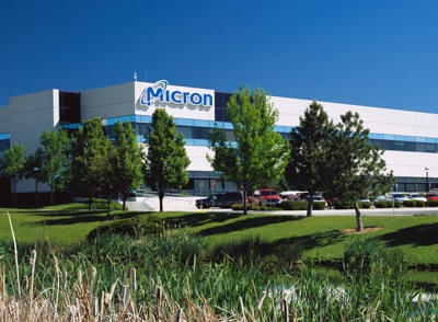
This is a Press Release edited by StorageNewsletter.com on August 24, 2017 at 3:01 pmMicron Technology, Inc. hosted an event at its HQs to mark the opening of a new facility which will play a critical role in the company’s research into new memory and storage technologies of the future.
When fully equipped, the new building will nearly double Micron’s cleanroom space dedicated to R&D in Boise, ID, and will support an expansion of the company’s overall R&D capabilities.
This expanded facility in Boise is the focal point for developing new semiconductor manufacturing processes and designs for the company’s future memory and storage technologies. Once developed in the Boise R&D center, these processes are then transitioned into production-scale manufacturing in Micron’s network of 12 large scale manufacturing plants (fabs) around the world.
Commemorating this milestone, Micron president and CEO, Sanjay Mehrotra, and technology development EVP, Scott DeBoer, guided public representatives and dignitaries through the new facility.
“Creating the world’s most advanced semiconductors is a highly complex process,” said Mehrotra. “The work done by our industry-leading team of scientists and engineers here in Idaho will help shape tomorrow’s technologies, products and solutions including future generations of phones, vehicles, and data centers, and advance rapidly emerging trends such as artificial intelligence and big data analytics. Today’s accomplishment of our R&D clean room space marks a significant acceleration of our innovation capabilities in Boise.“
Construction of the new clean-room facility began in October 2015 to create an expanded pristine, precision-controlled environment for development and fabrication of advanced memory integrated circuits leveraging Micron’s years of deep technical expertise. The foundation of the building required 24,000 cubic yards of concrete, the equivalent of a concrete truck delivery every hour for 100 days straight. Ten million pounds of steel were used to house this advanced research center, and the structure contains 240 miles of wire in the building alone, enough to reach the International Space Station.
The Boise R&D fab lies at the heart of Micron’s network of innovation, and its expansion will help accelerate the development of future generations of DRAM, NAND and emerging memory technologies.
DeBoer highlighted that Micron’s DRAM technology (1Ynm) has transitioned from Boise R&D and into Micron’s production fab in Hiroshima, Japan. Over the past year, the R&D team has also completed the development process in Boise for 64-layer 3D NAND, and moved the technology from initial development in Boise all the way through to volume production in Micron’s Singapore fabs.
In its role as the company’s technology development center, Boise R&D is leading the development of the next-generation of technologies such as future DRAM, 3D XPoint and 3D NAND.


 Subscribe to our free daily newsletter

