


Toshiba: QLC BiCS Flash 3D Memory With 4-Bit-Per-Cell …
Achieves capacity of 1.5TB in single package.
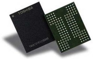
This is a Press Release edited by StorageNewsletter.com on July 4, 2017 at 2:21 pmToshiba America Electronic Components, Inc. (TAEC) announced the latest generation of its BiCS Flash three-dimensional (3D) flash memory (1).
This BiCS Flash device features 4-bit-per-cell, quadruple-level cell (QLC) technology and is the first (2) 3D flash memory device to do so. QLC technology enables larger (768Gb) die capacity than the company’s third-generation 512Gb 3-bit-per-cell, TLC, and pushes the boundaries of flash memory technology.
QLC BiCS Flash device features a 64-layer stacked cell structure and achieves the world’s largest die capacity (3) (768Gb/96GB). QLC flash memory also enables a 1.5TB device with a 16-die stacked architecture in a single package – featuring the industry’s largest capacity (4). This is a 50% increase in capacity per package when compared to firm’s earlier announcement of a 1TB device with a 16-die stacked architecture in a single package – which also offered the largest capacity in the industry at the time.
The technical challenges posed by QLC technology needed to be overcome, as increasing the number of bits-per-cell by one within the same electron count requires twice the accuracy of TLC technology. The company has combined its circuit design and leading 3D flash memory process technology to overcome this challenge, creating the world’s first QLC 3D flash memory.
The timing of this achievement is especially beneficial to datacenters.
“The introduction of QLC technology sets the stage for solving many of the challenges facing datacenters today,” noted Greg Wong, founder and principal analyst, Forward Insights. “For datacenters, QLC SSDs can be an excellent design choice for reducing power consumption and lowering footprint. Additionally, as the push for higher capacity HDDs leads to an increase in areal density and drives up the weight per successive generation, it has become common to see a 42U rack only half-filled due to exceeding maximum weight or power supply. Flash memory-based storage solutions weigh less and realize improved power efficiencies, enabling datacenters to achieve maximum rack capacity.“
The company was among the first to produce 64-layer 256Gb (32GB) devices. It was the first company to publically discuss QLC technology (at last year’s Flash Memory Summit) and it has long been a part of the company’s roadmap strategy for high-density, smaller chip size flash memory solutions. The new QLC device is targeted to applications including enterprise and consumer SSDs, tablets and memory cards.
“From SLC to MLC and MLC to TLC, large technology shifts are often met by industry resistance and the introduction of QLC is no exception,” noted Scott Nelson, SVP, memory business unit, TAEC. “There will always be demand for compelling storage solutions that bring higher densities and produce a favorable cost/performance equation – our QLC technology falls squarely into that sweet spot. History has proven us right in the past when it comes to our visionary flash memory roadmap, and we fully expect QLC BiCS FLASH to continue our industry-leading track record.“
Samples of company’s QLC device began shipping earlier in June to SSD and SSD controller vendors for evaluation and development purposes. Additionally, samples will be showcased at the 2017 Flash Memory Summit, taking place from August 7-10 in Santa Clara, CA.
Resources:
Technology Moves
Toshiba Memory Blog
[1] A structure stacking flash memory cells vertically on a silicon substrate to realize significant density improvements over planar NAND Flash memory, where cells are formed on the silicon substrate.
[2] As of June 28, 2017. Toshiba survey.
[3] As of June 28, 2017. Toshiba survey.
[4] As of June 28, 2017. Toshiba survey.


 Subscribe to our free daily newsletter

