


… And Prototype of 96-Layer BiCS Flash 3D With TLC …
Scheduled for release in second half of 2017 and mass production is targeted for 2018.
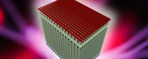
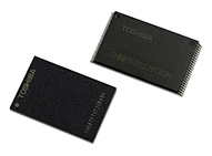
This is a Press Release edited by StorageNewsletter.com on July 4, 2017 at 2:17 pmToshiba Memory Corporation developed a prototype sample of 96-layer BiCS Flash three-dimensional (3D) flash memory with a stacked structure (1), with 3-bit-per-cell (TLC) technology.
Samples of this 96-layer product, which is a 256Gb (32GB) device, are scheduled for release in the second half of 2017 and mass production is targeted for 2018. These device meets market demands and performance specifications for applications that include enterprise and consumer SSD, smartphones, tablets and memory cards.
Going forward, the company will apply its 96-layer process technology to larger capacity products such as 512Gb (64GB) and 4-bit-per-cell (quadruple-level cell, QLC) technology in the near future.
The 96-layer stacking process combines with circuit and manufacturing process technology to achieve a capacity increase of approximately 40% per unit chip size over the 64-layer stacking process. It reduces the cost per bit, and increases the manufacturability of memory capacity per silicon wafer.
Since announcing the world’s first (2) prototype 3D flash memory technology in 2007, the company has continued to advance development of 3D flash memory and is promoting BiCS Flash to meet demand for larger capacities with smaller die sizes.
This 96-layer BiCS Flash will be manufactured at Yokkaichi Operations in Fab 5, the new Fab 2, and Fab 6, which will open in summer 2018.
(1) A structure stacking flash memory cells vertically on a silicon substrate to realize significant density improvements over planar NAND flash memory, where cells are formed on the silicon substrate.
(2) Source: Toshiba Memory Corporation, as of June 12, 2007.


 Subscribe to our free daily newsletter

