


Samsung in Volume Production of 64-Layer, 256Gb V-NAND Flash Memory
For server, PC and mobile applications, data transfer speed of 1Gb/s
This is a Press Release edited by StorageNewsletter.com on June 23, 2017 at 2:21 pmSamsung Electronics Co., Ltd. begun volume production of 64-layer, 256Gb V-NAND flash memory for use with an expanding line-up of storage solutions for server, PC and mobile applications.
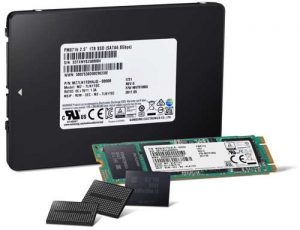
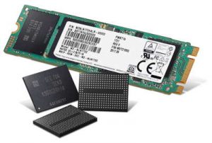
64-layer V-NAND product line-up
Since the company began producing the first SSDs based on 64-layer 256Gb V-NAND chips in January for key IT customers, it has been working on a range of V-NAND-based mobile and consumer storage solutions. These include embedded UFS memory, branded SSDs and external memory cards, which the company plans to introduce later this year.
To solidify its competitive edge in the memory market, the firm intends for its volume production of the 64-layer V-NAND chip, which is widely referred to as 4th generation V-NAND, to cover more than 50% of its monthly NAND flash production by year end.
“Following a long commitment to innovative technology, we will continuously push the limits of generations of industry-first V-NAND production, in moving the industry closer to the advent of the terabit V-NAND era,” said Kye Hyun Kyung, EVP, flash product and technology team, memory business, Samsung Electronics. “We will keep developing next-generation V-NAND products in sync with the global IT industry so that we can contribute to the timeliest launches f new systems and services, in bringing a higher level of satisfaction to consumers.“
The company’s 64-layer 3-bit 256Gb V-NAND features a data transfer speed of 1Gb/s, which is the fastest among currently available NAND flash memory. Also, it has the industry’s shortest page program time (tPROG) (*) of 500㎲ among NAND flash memory, which is about four times faster than that of a typical 10nm class (**), planar NAND flash memory and approximately 1.5 times faster than that of firm’s fastest 48-layer 3-bit 256Gb V-NAND flash.
With today’s ample supply of V-NAND products, the firm expects that the industry will now focus more on the high performance and reliability of memory storage, rather than immerse itself in a chip scaling race.
The 64-layer 256Gb V-NAND provides more than a 30% productivity gain, compared to the 48-layer 256Gb V-NAND that preceded it. In addition, the 64-layer V-NAND has a 2.5V input voltage for its circuits, which leads to approximately 30% greater energy efficiency than the 3.3 volts that 48-layer V-NAND used. Also, the reliability of the new V-NAND cell increased by about 20% compared to its predecessor.
The company enabled these improvements by tackling a diversity of challenges that appear in the advanced V-NAND manufacturing process. Chief among them were realizing multi-billion channel holes that penetrate several dozen layers of cell-arrays, and minimizing the loss of electrons from about 85.3 billion cells.
As the layers of cell arrays increase, the level of technological difficulty also increases, especially in making the channel holes homogeneous in their shape from the top to the bottom layer, and in properly dispersing the weight of all the layers to improve the stability of the channel holes.
Another challenge that the company overcame was to realize 64 layers of cell arrays based on 3D CTF (Charge Trap Flash) structure and uniformly cover the inner side of each channel hole with an atomically thin, non-conductive substance. This led to the creation of smaller cells with improved performance and reliability.
Based on 15 years of research into its proprietary V-NAND 3D structure, the firm has formed the basis for more than 500 patents related to essential technological findings, and filed applications for them in many countries including Korea, the U.S. and Japan. Based on its success with 64-layer V-NAND, the company has secured the fundamental technology that it needs in the future to produce V-NAND chips with one terabit capacity and more, by stacking over 90 layers of cell arrays.
(*) Note: Page program time (tPROG) refers to the period of time that it takes to record data on a designated cell. It is a key parameter that determines the write performance of a NAND flash memory chip.
(**) Note: 10nm-class is a process technology node somewhere between 10 and 20nm.


 Subscribe to our free daily newsletter

