


NAND Vendors Put All Chips on TLC 3D NAND – Wikibon
3D XPoint not be adopted in volume.
This is a Press Release edited by StorageNewsletter.com on June 23, 2017 at 2:22 pm This article was published on June 6, 2017 by David Floyer, research analyst at Wikibon, Inc.
NAND Vendors puts all their chips on TLC 3D NAND
Premise
By mid 2018, 3D NAND will become the backbone of almost all deliveries and all vendors of NAND flash, to both the consumer and enterprise markets, with a clear path to increased density, higher performance, and decreasing cost. Consumer NAND announcements are a leading indicator of enterprise NAND capabilities.
Table 1 – Toshiba Consumer SSD NAND Announcement
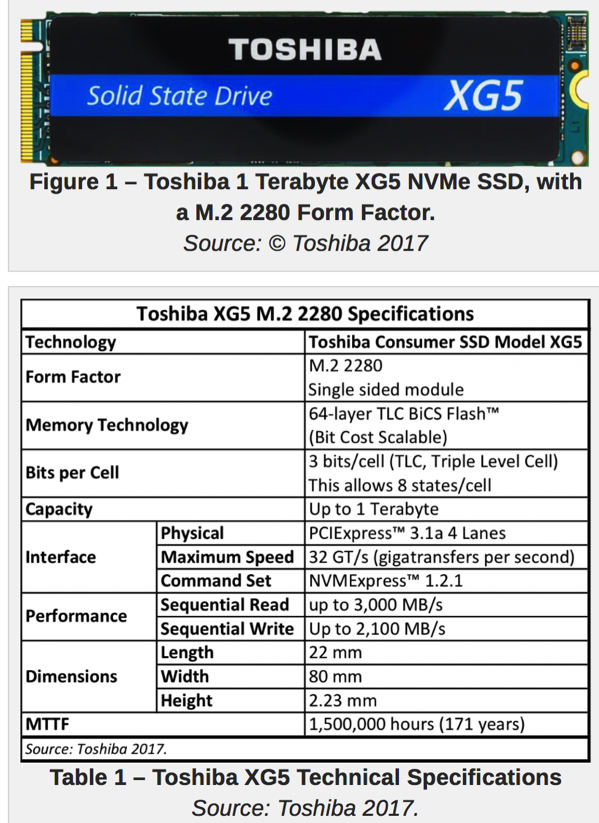
Toshiba is first out of the gate with an announced product deploying 64-layers. It has announced that the XG5 SSD has qualified its 3D NAND technology with consumer OEM partners, and will be shipping to Dell and others. Table 1 shows the form factor as a single-sided M.2 2280. It uses the high speed NVMe protocol to connect to Gen 3 PCIe.
The 3D NAND technology utilized is 64-layer, using TLC (TLC, allows 8 states/cell). It competes with products such as the Samsung 960 Pro M.2 1TB or two-sided 2TB NVMe Gen 3 drive at a retail cost of about $500/TB.
This drive form factor can be used in mainstream PCs, thin performance notebooks, enthusiast desktop and laptops. It has potential use in servers for storing BIOS, configuration, and other server management functions.
The technical specifications are shown in Table 1. The bit density is a function of the number of layers, and the bits/cell. Of interest is the attachment to the PCIe Gen 3 bus, which is much faster than SAS or SATA connections. The NVMe protocol is also more efficient than the SCSI protocol. This leads to sequential read rate of 3GB/s, and sequential writes of about 2GB/s.
Of significant interest is the MTTF, mean time to failure, of 1.5 million hours.
Table 2 -Toshiba Strategy for Enterprise 3D NAND
With consumer performance of this capability, it is clear that this technology will also be used in the enterprise space, mainly in the 2.5-inch SSD form factor. Wikibon also projects that attaching directly to the PCIe bus on the server will be the preferred configuration; traditional SATA and SAS connections are now be too slow to compete. The NVMe protocol will also be an obvious choice for 3D NAND, and much faster than the traditional SCSI connection.
Wikibon understands that Toshiba plans to migrate all of its 2D NAND flash product lines over to 3D TLC NAND by early 2018. The firm have a strong partnership with Western Digital for NAND fabs. Wikibon expects that design wins and enterprise OEM agreements for SSDs and other form factors will be completed by the end of 2017, and be in full volume production late 2017/early 2018.
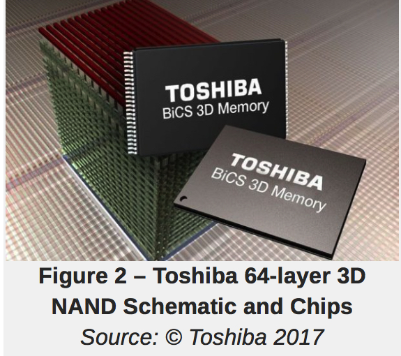
Toshiba plans to migrate all the fabs from 2D to 3D. 3D allows multiple layers of cells to added vertically, and increases the number of cells/chip (see Table 2).
General Migration to 3D NAND
All the NAND manufacturers have announced plans to aggressively move from 2D to 3D NAND. Samsung was the first NAND vendor to deliver 3D NAND flash in volume in 2016, deploying 48 layers. Samsung plans to move to 64 layers.
Toshiba has moved from 48 layers in the 3D stack to 64 layers, and the XG5 is the first product to be released with 64 layers. Toshiba will be moving to 72 layers, 96 layers, and then 128 layers.
Toshiba and Western Digital in partnership have developed the BiCS (Bit Cost Scalable) 3D NAND technology, using charge-trap technology developed by Toshiba. Samsung uses a charge-trap V-NAND technology, along with SK Hynix; SF Hynix has plans to move to 72 layers by end 2017. The Micron/Intel uses a floating-gate 3D NAND technology.
All vendors are moving to TLC NAND. Toshiba looks as if will be the first to actually deliver TLC OEM products this summer (2017). TLC NAND reads and writes 3 bits/cell. This offers 8 states per cell, compared with 4 states for MLC NAND, and 2 states (on/off, 1/0) for SLC NAND. Toshiba enterprise products will also be using TLC. Toshiba is confident that the technology is robust enough for enterprise use, and the MTTF figure of 1,500,000 hours (171 years) in Table 1 seems to confirm that.
Toshiba and other vendors will be driving to implement QLC (quad-level cell), which as the name suggests is four bits/cell, sixteen states/cell. This again will double the amount of information held per cell, compared to TLC.
The investments in NAND technologies in both density and volume are likely to increase shipments, and return cost reductions to those projected by Moore’s law. NAND technology has had many nay-sayers, who have argued that new generations of NAND would be unable to meet enterprise needs. As usual, the inventiveness of engineers and the drive of the very large consumer market for NAND storage have won out, and NAND looks to be set for another decade. 3D NAND technology will drive very high volumes and densities, and Wikibon projects it will drive mechanical magnetic HDD technologies almost completely out of the consumer space in the next 5 years. HDDs will be around for longer in the enterprise space, but increasingly in back-end and archive roles.
NAND prices have stayed high, and increased over the past two quarters. This has had a positive result for revenue and profits from all NAND vendors. This increase in price before a new level of technology starts to ship in volume is common. Perhaps most importantly of all, the confidence and profits in the industry have insured the investments necessary to fund the new fabs have been forthcoming.
Wikibon expect NAND prices to fall, as 3D volume shipments from all manufacturers ramp up in late 2017. This rise and fall is typical of technology migrations in both the DRAM and NAND memory markets.
NAND technology together with DRAM looks set to continue to dominate computing for the foreseeable future.
Impact of DRAM Memory Technology
DRAM has also been in short supply, along with NAND, causing prices to rise and memory vendors to enjoy higher revenues and profits. One important system impact of NAND is to increase the amount of I/O and data that moves to and from storage. The impact is that a balanced system with NAND storage should have more DRAM. The increase in DRAM and NAND has the ability to increase processor utilizations up from the current anaemic 10% average utilization. This more than cost justifies the additional DRAM and NAND.
The second area of innovation is the creation of hybrid DRAM/flash DIMMs. This is sometimes called storage class memory (SCM). This was an area that many thought would belong to DRAM together with 3D XPoint; however Wikibon’s research entitled Will 3D XPoint make it? indicates this is very unlikely to happen. The first DRAM/NAND hybrid in this area was Diablo in conjunction with SanDisk (now Western Digital). The NAND flash acts as a very fast SATA disk, in support of system paging and other system processes.
Another approach is taken by Netlist Inc, with a new HybriDIMM Storage Class Memory (SCM). It describes it as the industry’s first standards-based, plug-and-play SCM solution based on an industry-standard DDR4 LRDIMM interface. This allows it to operate in current Intel x86 servers without BIOS or hardware changes. They also claim data management software allows the DRAM/NAND hybrid to operate as very large DRAM (up to 1TB) in storage, with average access times below 1 microsecond. This type of hybrid technology may be very useful for stateless bid-data databases such as MongoDB. Netlist has a partnership with Samsung.
Wikibon Projects 3D XPoint Will not Be Adopted in Volume
3D XPoint is a PCM technology developed by Intel and Micron. It came onto the scene in 2015 with a bang, promising 1,000 times the speed, 1,000 time the durability of NAND, with a density 10 times greater than DRAM. The analysis in Wikibon research entitled Will 3D XPoint make it? demonstrates that 3D NAND has almost overtaken the specifications of 3D XPoint, at much higher densities and lower price-points. Wikibon projects it is unlikely that 3D XPoint will be used extensively in either consumer or enterprise computing.
3D NAND Enables ‘UniGrid’ Architecture
The good news is that the groundbreaking work that Intel and SNIA drove in creating great NVMe and NVMe over Fabric specifications for 3D XPoint has provided the basis of standards for much faster computers based on multiple processor nodes, large DRAM, and 3D NAND interconnected with very fast 100GbE networks, mainly from Mellanox.
Micron recently announced such an architecture called SolidScale, based on a NVMesh technology that Micron is OEMing from Excelero. Wikibon is coining the work ‘UniGrid’ to describe this system architecture, which is set to revolutionize the next generation of applications.
Action Item
CIOs and CTO should assume that 3D NAND and DRAM will remain the dominant consumer and enterprise memory technologies for the foreseeable future, with 3D NAND providing the persistence layer for most data, DRAM in different configurations providing some persistence for smaller amounts of data. The most exciting and disruptive outcome of this 3D NAND disruption is the emergence of the ‘UniGrid’ system architecture, which will revolutionize the next generation of applications.


 Subscribe to our free daily newsletter

