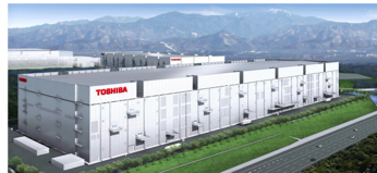
Toshiba Starts Construction of Fab 6 and Memory R&D Center at Yokkaichi, Japan
For 3D flash memory
This is a Press Release edited by StorageNewsletter.com on February 10, 2017 at 2:48 pmToshiba Corporation has started construction of a new semiconductor fabrication facility, Fab 6, and a new R&D center, the Memory R&D Center, at Yokkaichi Operations in Mie prefecture, Japan, the company’s main memory production base.

Fab 6 will be dedicated to production of BiCS FLASH, Toshiba’s 3D flash memory (1). Like Fab 5, construction will take place in two phases, allowing the pace of investment to be optimized against market trends, with completion of Phase 1 scheduled for summer 2018. The company will determine installed capacity and output targets and schedules by monitoring the market.
Toshiba will also construct a Memory R&D Center adjacent to the new fab, with completion targeting December 2017. The facility will advance development of BiCS FLASH and new memories.
(1) A structure that stacks flash memory cells on a silicon substrate. It realizes significant density improvements over planar NAND flash memory, where cells are formed on the substrate.


 Subscribe to our free daily newsletter

