


R&D: Memory Device Sees Light
Ferroelectric tunnel junction promises low-power, high-density data storage.
This is a Press Release edited by StorageNewsletter.com on August 1, 2016 at 3:10 pmFrom King Abdullah University of Science and Technology
An electronic device that could lead to smaller, low-power memory chips can now be controlled and probed by light, as revealed by research from KAUST (King Abdullah University of Science and Technology).
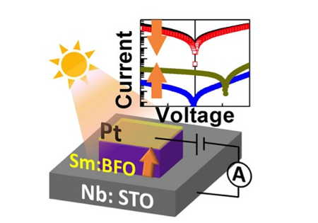
A ferroelectric tunnel junction made from platinum (Pt) samarium-doped
bismuth iron oxide (Sm:BFO) and niobium-doped strontium titanate (Nb:STO)
is a memory device that can be controlled by both electricity and light.
(© 2016 KAUST)
The device is a ferroelectric tunnel junction (FTJ) that contains a thin layer of a ferroelectric material sandwiched between two electrodes. Ferroelectric materials are intrinsically polarized so that negative electrical charge concentrates on one side of the layer and positive charge clusters on the opposite side. Applying an electric field flips this polarization, and the two states can represent the ‘1’s and ‘0’s of binary data. The device crucially does not need power to retain this data.
Tom Wu of from the KAUST Material Science and Engineering program and colleagues created an FTJ containing a film of ferroelectric samarium-doped bismuth iron oxide (SBFO) that was just three to nine nanometers thick. One electrode was made of platinum and the other was niobium-doped strontium titanate (NSTO), a light-sensitive semiconductor.
Electrons can sometimes tunnel through a very thin ferroelectric layer – a quantum mechanical process that allows them to skip across an energy barrier to create a current. In one of its polarization states, SBFO has a low tunneling electroresistance (TER) that allows electrons across. However, in the other polarization state, the team found that its TER is 100,000 times larger, which prevents electron tunneling. This is the largest change in TER ever seen for a FTJ, providing an unambiguous way to read its polarization state.
Exposing the device to ultraviolet light reduced this high TER ten-fold, as light makes NSTO more conducting, which assists electron tunneling.
“This means that we could acquire a total of four electronic states corresponding to polarization direction (left or right) and illumination condition (dark or light),” noted Wu. “Each electronic state can be used to store one bit of information. By introducing light illumination into FTJs, we double the data storage density, which could be very promising for future technology.”
Although the TER difference between the two states gradually wanes, the team calculated that there would still be a significant distinction after 10 years, making it suitable for long-term data storage.
It took about ten microseconds to switch the device from one state to the other – faster than conventional flash memory but lower than some other forms of advanced memory.
“One immediate goal of our research is to make these FTJ devices smaller and faster,” said Wu. “In addition, we will work to enhance the light detection capability of such ultrathin junctions.”
Article:
Optically controlled electroresistance and electrically controlled photovoltage in ferroelectric tunnel junctions
Nature Communications has published an article written by Wei Jin Hu, Materials Science and Engineering, King Abdullah University of Science and Technology (KAUST), Thuwal 23955-6900, Saudi Arabia, Zhihong Wang, Advanced Nanofabrication Core Lab, King Abdullah University of Science and Technology (KAUST), Thuwal 23955-6900, Saudi Arabia, Weili Yu, and Tom Wu, Materials Science and Engineering, King Abdullah University of Science and Technology (KAUST), Thuwal 23955-6900, Saudi Arabia
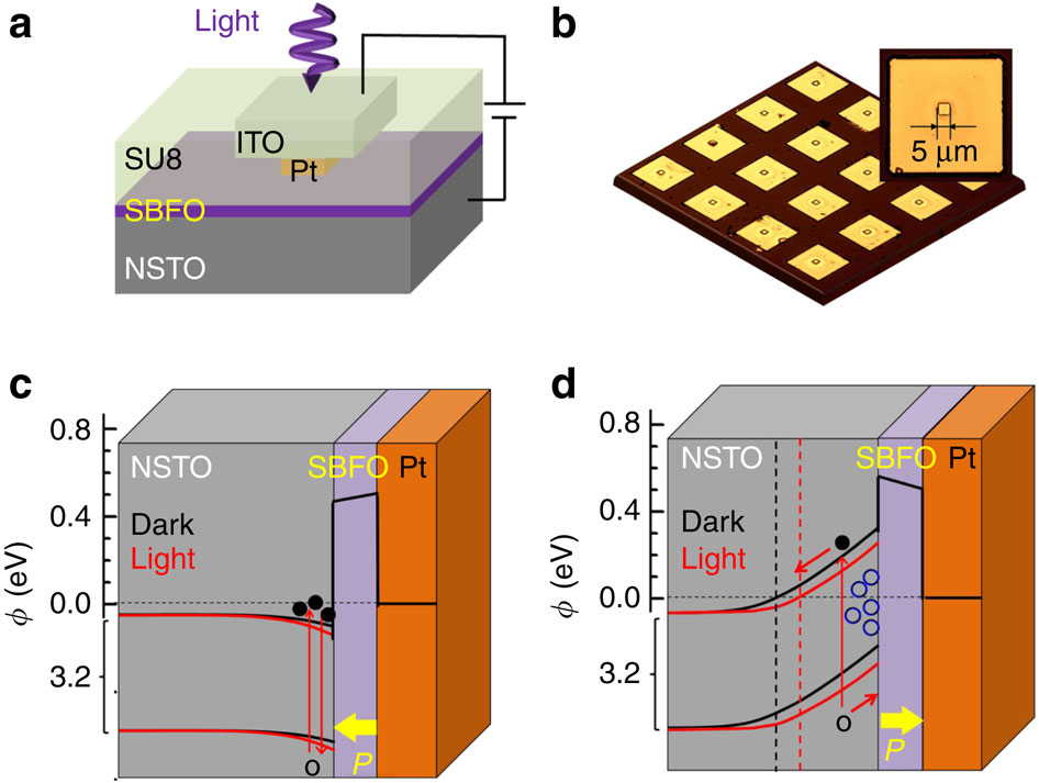
(a) Schematic representation of structure of the NSTO/SBFO/Pt FTJs.
(b) Optical image of the as-prepared FTJs with an effective junction area of 5 μm × 5 μm
(shown in the inset). Band alignment in the dark and under light illumination are shown
for ferroelectric polarization (yellow arrow) pointing to either
(c) the semiconducting NSTO electrode or (d) the metal electrode Pt.
Polarization-modified carrier accumulation/depletion at the NSTO/SBFO
interface contributes to the complementary electroresistance and PV effects.
Electric-filed-induced drift of positively charged oxygen vacancies (blue circles)
from the NSTO bulk towards the interface is also illustrated in d.
Black filled (empty) circles represent photon-excited electrons (holes).
Abstract: “Ferroelectric tunnel junctions (FTJs) have recently attracted considerable interest as a promising candidate for applications in the next-generation non-volatile memory technology. In this work, using an ultrathin (3 nm) ferroelectric Sm0.1Bi0.9FeO3 layer as the tunnelling barrier and a semiconducting Nb-doped SrTiO3 single crystal as the bottom electrode, we achieve a tunnelling electroresistance as large as 105. Furthermore, the FTJ memory states could be modulated by light illumination, which is accompanied by a hysteretic photovoltaic effect. These complimentary effects are attributed to the bias- and light-induced modulation of the tunnel barrier, both in height and width, at the semiconductor/ferroelectric interface. Overall, the highly tunable tunnelling electroresistance and the correlated photovoltaic functionalities provide a new route for producing and non-destructively sensing multiple non-volatile electronic states in such FTJs.“


 Subscribe to our free daily newsletter

