


R&D: IBM Scientists Achieve Storage Memory Breakthrough With Phase-Change
Three bits per cell in 64k-cell array at elevated temperatures and after one million endurance cycles
This is a Press Release edited by StorageNewsletter.com on May 25, 2016 at 2:59 pmScientists at IBM Research have demonstrated reliably storing three bits of data per cell using a relatively new memory technology known as phase-change memory (PCM).
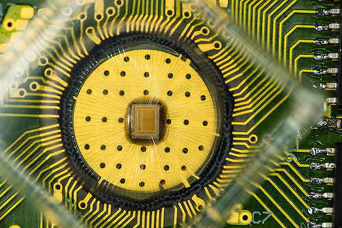
The chip consists of a 2×2 Mcell array with a 4-bank interleaved architecture.
The memory array size is 2×1000μm×800μm. The PCM cells are based
on doped-chalcogenide alloy and were integrated into the prototype chip
serving as a characterization vehicle in 90nm CMOS baseline technology.
(Credit: IBM Research)
The current memory landscape spans from venerable DRAM to HDD drives to ubiquitous flash. But in the last several years PCM has attracted the industry’s attention as a potential universal memory technology based on its combination of R/W speed, endurance, non-volatility and density. For example, PCM doesn’t lose data when powered off, unlike DRAM, and the technology can endure at least 10 million write cycles, compared to an average flash USB stick, which tops out at 3,000 write cycles.
This research breakthrough provides fast and easy storage to capture the exponential growth of data from mobile devices and the Internet of Things.
Applications
IBM scientists envision standalone PCM as well as hybrid applications, which combine PCM and flash storage together, with PCM as an extremely fast cache. For example, a mobile phone’s OS could be stored in PCM, enabling the phone to launch in a fews. In the enterprise space, entire databases could be stored in PCM for blazing fast query processing for time-critical online applications, such as financial transactions.
Machine learning algorithms using large data sets will also see a speed boost by reducing the latency overhead when reading the data between iterations.
How PCM Works
PCM materials exhibit two stable states, the amorphous (without a clearly defined structure) and crystalline (with structure) phases, of low and high electrical conductivity, respectively.
To store a ‘0’ or a ‘1’, known as bits, on a PCM cell, a high or medium electrical current is applied to the material. A ‘0’ can be programmed to be written in the amorphous phase or a ‘1’ in the crystalline phase, or vice versa. Then to read the bit back, a low voltage is applied. This is how re-writable Blue-ray discs store videos.
Previously scientists at IBM and other institutes have successfully demonstrated the ability to store 1 bit per cell in PCM, but at the IEEE International Memory Workshop in Paris, France, IBM scientists presented for the first time successfully storing three bits per cell in a 64k-cell array at elevated temperatures and after one million endurance cycles.
“PCM is the first instantiation of a universal memory with properties of both DRAM and flash, thus answering one of the grand challenges of our industry,” said Dr. Haris Pozidis, author of the paper and manager of non-volatile memory research, IBM Research – Zurich. “Reaching three bits per cell is a significant milestone because at this density the cost of PCM will be less than DRAM and closer to flash.“
To achieve multi-bit storage IBM scientists have developed two innovative enabling technologies: a set of drift-immune cell-state metrics and drift-tolerant coding and detection schemes.
More specifically, the new cell-state metrics measure a physical property of the PCM cell that remains stable over time, and are thus insensitive to drift, which affects the stability of the cell’s electrical conductivity with time. To provide additional robustness of the stored data in a cell over ambient temperature fluctuations a novel coding and detection scheme is employed. This scheme adaptively modifies the level thresholds that are used to detect the cell’s stored data so that they follow variations due to temperature change. As a result, the cell state can be read reliably over long time periods after the memory is programmed, thus offering non-volatility.
“Combined these advancements address the key challenges of multi-bit PCM, including drift, variability, temperature sensitivity and endurance cycling,” said Dr. Evangelos Eleftheriou, IBM fellow.
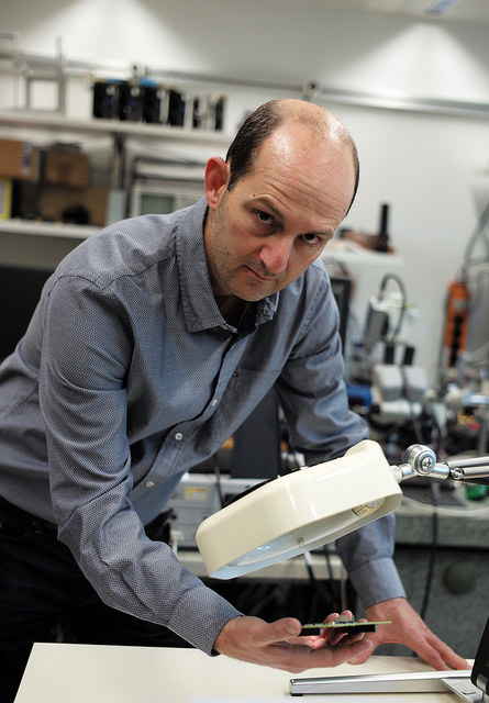
IBM scientist , Nikolaos Papandreou holds
the PCM chip under a magnifying lens in his lab.
The experimental multi-bit PCM chip used by scientists is connected to a standard integrated circuit board. The chip consists of a 2×2 Mcell array with a 4-bank interleaved architecture. The memory array size is 2 ×1000μm ×800μm. The PCM cells are based on doped-chalcogenide alloy and were integrated into the prototype chip serving as a characterization vehicle in 90nm CMOS baseline technology.
OpenPOWER
At the 2016 OpenPOWER Summit in San Jose, CA, last month, IBM scientists demonstrated for the first time phase-change memory attached to POWER8-based servers (made by IBM Corp. and TYAN Computer Corp.) via the CAPI (Coherent Accelerator Processor Interface) protocol. This technology leverages the low latency and small access granularity of PCM, the efficiency of the OpenPOWER architecture and the CAPI protocol. In the demonstration the scientists measured very low and consistent latency for 128-byte R/Ws between the PCM chips and the POWER8 processor.
Video from IBM Research
Papers:
- Demonstration of Reliable Triple-Level-Cell (TLC) Phase-Change Memory by M. Stanisavljevic, H. Pozidis, A. Athmanathan, N. Papandreou, T. Mittelholzer, and E. Eleftheriou,”D” in Proc. International Memory Workshop, Paris, France, May 16-18, 2016
- Multilevel-Cell Phase Change Memory: A Viable Technology by Aravinthan Athmanathan, Milos Stanisavljevic, Nikolaos Papandreou, Haralampos Pozidis and Evangelos Eleftheriou.


 Subscribe to our free daily newsletter

