


Winbond Introduces SpiStack Flash Memories in 8-Pin Packages
Devices offer flexibility in combining densities for variety of applications
This is a Press Release edited by StorageNewsletter.com on April 1, 2016 at 3:01 pmWinbond Electronics Corporation announced an expansion of its flash product portfolio with the introduction of a family of stackable SpiFlash memories.
 The SpiStack W25M Series is company’s first to allow the ‘stacking’ of homogeneous or heterogeneous flash, thus achieving memories of varying densities for code and/or storage, while providing designers with the flash solutions most appropriate for their design requirements.
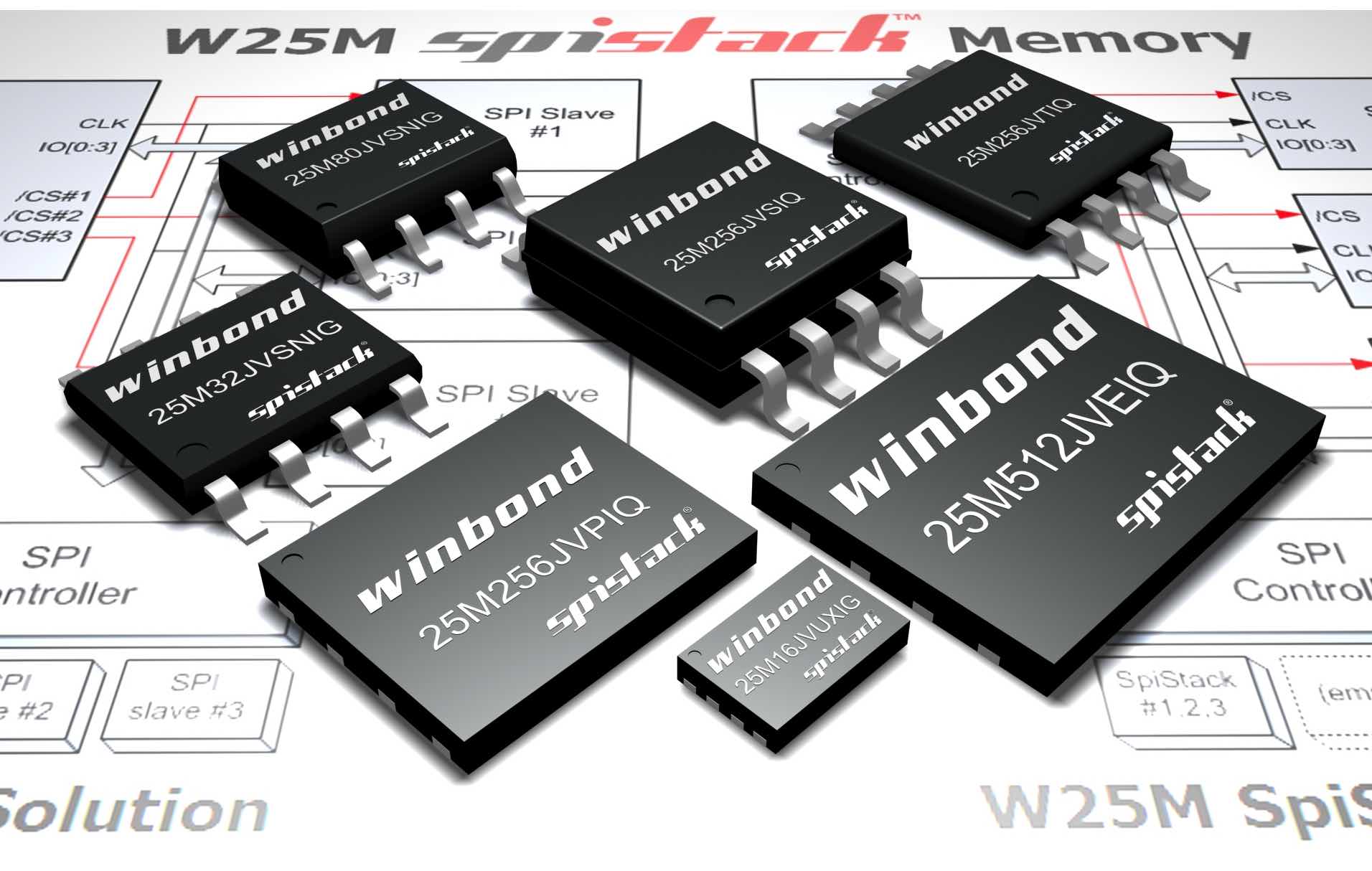
The W25M Series provides a range of densities in the well-established 8-pin package to which designers are accustomed. Additionally, W25M memories feature the multi-IO SpiFlash interface and command set.
“Stacking memories, both homogeneously and heterogeneously, is a revolutionary method of creating optimal memory solutions,” said Mike Chen, director, technical marketing, Winbond Electronics Corporation America. “Winbond developed the SpiStack architecture to give designers maximum flexibility in tailoring flash solutions to meet their specific memory-density and -application requirements.”
SpiStack homogeneous memories are achieved by stacking SpiFlash dies – for example, two 256Mb dies combining to form a single SpiFlash 512Mb NOR memory – in the industry-standard 8-pin 8x6mm WSON package. This stacked product, W25M512JV, is also available in the widely used 16-pin SOIC or 24-pad BGA packages and is sampling. SpiStack heterogeneous memories call for the stacking of a NOR memory with a NAND die, such as a 64Mb SpiFlash NOR blended with a 1Gb Serial NAND die, which gives designers the flexibility to store code in the NOR die and data in the NAND memory.
SpiStack highlights:
-
Multiple SpiFlash dies, each with density ranging from 16Mb to 2Gb, can be stacked with any combination of NOR and NAND dies.
-
Each die can be used according to its specifically beneficial characteristics. A NOR die can be used to store the boot code, thanks to its cell characteristics that deliver better endurance and retention, and fast random access time. A NAND memory can be used to store data and/or to backup the boot code.
-
A NAND die can be used to upload the working memory data quickly whenever the system power goes down, thanks to its programming time that’s much faster than NOR. It improves the system quality by storing up-to-date code residing in the working memory for later usage.
-
SpiStack supports concurrent operation so that code execution is not interrupted for data updates.
-
All SpiStack features are supported in an 8-pin package along with the standard QSPI command, so that backward compatibility is conserved. This is done with the addition of a simple software die select instruction (C2h) and a factory-assigned die ID number. The dies are stacked based on Winbond’s unique stacking process technology.
To ensure satisfying the growing global demand for high-volume solutions, SpiFlash memories are manufactured in the company’s 12-inch wafer fabrication facility in Taichung, Taiwan.
The SpiStack flash memory solutions are sampling and being designed-in, and will be available in volume production starting 2Q16.


 Subscribe to our free daily newsletter

