


Graphene Key to High-Density, Energy-Efficient Memory Chips, Stanford Engineers Say
R&D: three Stanford University projects to create data storage technologies that use nanomaterials other than standard silicon.
This is a Press Release edited by StorageNewsletter.com on October 28, 2015 at 2:52 pmOnly an atom thick, graphene is a key ingredient in three Stanford University projects to create data storage technologies that use nanomaterials other than standard silicon.
By Ramin Skibba
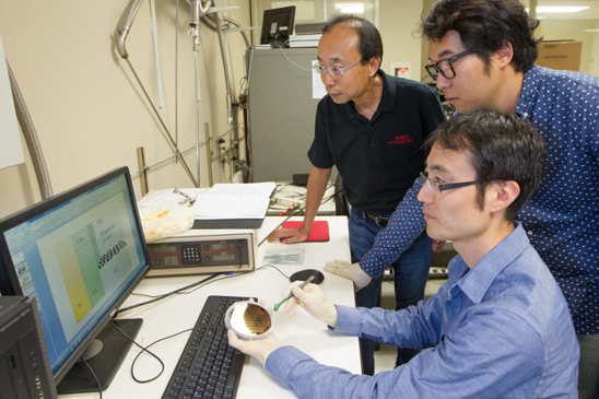
Professor H.-S. Philip Wong, left, graduate student Joon Sohn
and postdoctoral fellow Seunghyun Lee (seated)
are developing high-capacity, energy-efficient memory chips
that are not based on silicon.
The memory chips in phones, laptops and other electronic devices need to be small, fast and draw as little power as possible. For years, silicon chips have delivered on that promise.
But to dramatically extend the battery life of mobile gadgets, and to create data centers that use far less energy, engineers are developing memory chips based on new nanomaterials with capabilities that silicon can’t match.
In three recent experiments, Stanford engineers demonstrate post-silicon materials and technologies that store more data per square inch and use a fraction of the energy of today’s memory chips.
The unifying thread in all three experiments is graphene, an extraordinary material isolated a decade ago but which had, until now, relatively few practical applications in electronics.
A purified relative of pencil lead, graphene is formed when carbon atoms link together into sheets just one atom thick. Atom-thin graphene is stronger than steel, as conductive as copper and has thermal properties useful in nanoscale electronics.
“Graphene is the star of this research,” said Eric Pop, associate professor of electrical engineering and a contributor to two of the three memory projects. “With these new storage technologies, it would be conceivable to design a smartphone that could store ten times as much data, using less battery power, than the memory we use today.“
Professor H.-S. Philip Wong and Pop led an international group of collaborators who describe three graphene-centric memory technologies in separate articles in Nature Communications, Nano Letters and Applied Physics Letters.
While consumers might appreciate the mobile application of these new technologies, engineers think post-silicon memory chips may also transform server farms that must store and deliver quick access to the vast quantities of data stored in the cloud.
“Data storage has become a significant, large-scale consumer of electricity, and new solid-state memory technologies such as these could also transform cloud computing,” Wong said.
Memory makeover
Memory chips store data as a string of ones and zeroes. Today most memory chips are based on silicon, and come in two basic types – volatile and non-volatile. Volatile memory, such as random access memory (RAM), offers fast but temporary storage. When the power shuts off, the zeros and ones vanish.
Non-volatile memory, such as the flash memory in cell phones, is slow but stable. Even if the battery expires the data remains.
The Stanford-led engineers show how to create memory with the speed of RAM and the persistence of flash by using new materials and technologies that require less energy than silicon to store the zeroes and ones.
In Nature Communications, Wong worked with postdoctoral fellow Seunghyun Lee and PhD candidate Joon Sohn on a technique known as resistive random-access memory, or RRAM for short.
In RRAM chips, tiny jolts of electricity switch certain metal oxides between resistive and conductive states. When the metal oxides resist the flow of electrons, that creates a zero. When the materials conduct electrons, that is a one. RRAM is fast, like volatile silicon memory, but like flash memory it retains stored data when the power is turned off.
This work demonstrates the possibility of constructing non-volatile RRAM while densely storing data without consuming more energy.
New phases of memory
In two other papers, published in Applied Physics Letters and Nano Letters, Pop and Wong led research teams that used graphene to make advances with a different but conceptually similar storage approach called phase-change memory.
In phase-change memory, a tiny jolt of electricity causes an alloy of germanium, antimony and tellurium to change its atomic structure. One jolt tweaks the atoms into a regular, crystalline structure that allows electrons to flow, notated as a digital one. A second jolt makes the structure irregular, or amorphous, creating a zero. Each jolt quickly toggles the phase-change material from one to zero. Like RRAM, it retains its stored data when the power is turned off.
In the Applied Physics Letters paper, Pop led a team that included former students at the University of Illinois Urbana-Champaign and collaborators at the Universities of Modena and Bologna in Italy. They used ribbons of graphene as ultra-thin electrodes to intersect phase-change memory cells, like skewers spearing marshmallows. This setup also exploited the atomically thin edge of graphene to push current into the material, and change its phase, again in an extremely energy-efficient manner.
In the Nano Letters paper, Pop and Wong used both the electrical and thermal properties of graphene in a phase-change memory chip. However, in a twist, here they used the surface of the graphene sheet to contact the phase-change memory alloy. In essence, the graphene prevented the heat from leaking out of the phase-change material, creating a more energy-efficient memory cell.
These studies show that graphene is far from a laboratory curiosity, Pop and Wong say. The material ‘s unique electrical, thermal and atomically thin properties can be utilized to create more energy-efficient data storage. Such properties do not exist in the silicon world, yet could potentially transform the way we store and access our digital data in the future.
References :
Metal oxide-resistive memory using graphene-edge electrodes
Nature Communications has published an article written by Seunghyun Lee, Joon Sohn, Zizhen Jiang, Hong-Yu Chen, and H.-S. Philip Wong, Department of Electrical Engineering and Stanford SystemX Alliance, Stanford University, Stanford, California 94305, USA
(a) An illustration of graphene-based RRAM in a vertical cross-point architecture. The RRAM cells are formed at the intersections of the TiN pillar electrode and the graphene plane electrode. The resistive switching HfOx layer surrounds the TiN pillar electrode and is also in contact with the graphene plane electrode. (b) A schematic cross-section of the graphene-based RRAM. (c) High-resolution TEM image (details in Methods section) of the two-stack GS-RRAM structure. The RRAM memory elements are highlighted in red. Scale bar, 40 nm. (d,e) First and second layer of GS-RRAM with graphene on top of the Al2O3 layer. Scale bars, 5 nm. (f,g) TEM image of the two-stack Pt-based RRAM from previous work. Scale bars, 40 nm (f) and 5 nm (g).
Click to enlarge
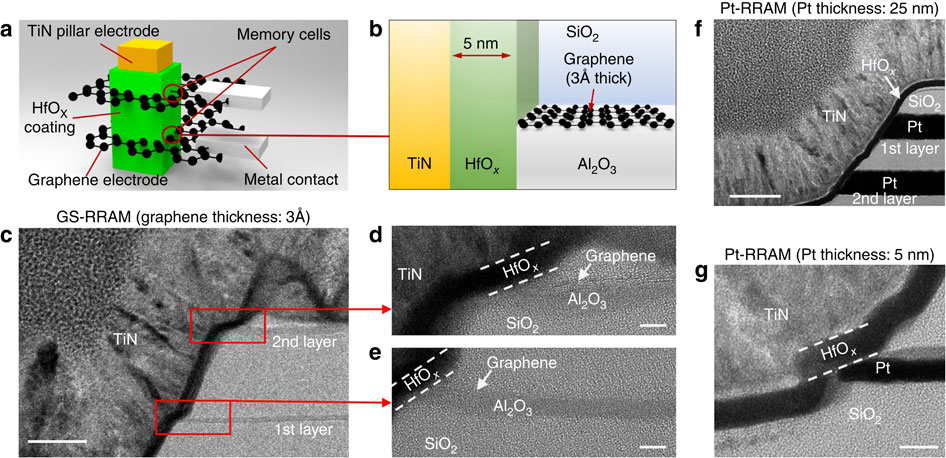
Abstract : “The emerging paradigm of ‘abundant-data’ computing requires real-time analytics on enormous quantities of data collected by a mushrooming network of sensors. Todays computing technology, however, cannot scale to satisfy such big data applications with the required throughput and energy efficiency. The next technology frontier will be monolithically integrated chips with three-dimensionally interleaved memory and logic for unprecedented data bandwidth with reduced energy consumption. In this work, we exploit the atomically thin nature of the graphene edge to assemble a resistive memory (~3 Å thick) stacked in a vertical three-dimensional structure. We report some of the lowest power and energy consumption among the emerging non-volatile memories due to an extremely thin electrode with unique properties, low programming voltages, and low current. Circuit analysis of the three-dimensional architecture using experimentally measured device properties show higher storage potential for graphene devices compared that of metal based devices.”
Energy-Efficient Phase-Change Memory with Graphene as Thermal Barrier
Nano Letters has published an article written by Chiyui Ahn†, Scott W. Fong†, Yongsung Kim‡, Seunghyun Lee†, Aditya Sood, Christopher M. Neumann†, Mehdi Asheghi§, Kenneth E. Goodson, Eric Pop†, and H.-S. Philip Wong†
†Department of Electrical Engineering, §Department of Mechanical Engineering, and ∥Department of Materials Science and Engineering, Stanford University, Stanford, California 94305, United States
‡ Samsung Advanced Institute of Technology (SAIT), Suwon, 443-803, South Korea
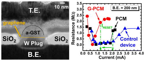
Abstract: “Phase-change memory (PCM) is an important class of data storage, yet lowering the programming current of individual devices is known to be a significant challenge. Here we improve the energy-efficiency of PCM by placing a graphene layer at the interface between the phase-change material, Ge2Sb2Te5 (GST), and the bottom electrode (W) heater. Graphene-PCM (G-PCM) devices have ∼40% lower RESET current compared to control devices without the graphene. This is attributed to the graphene as an added interfacial thermal resistance which helps confine the generated heat inside the active PCM volume. The G-PCM achieves programming up to 105 cycles, and the graphene could further enhance the PCM endurance by limiting atomic migration or material segregation at the bottom electrode interface”
Nanoscale phase change memory with graphene ribbon electrodes
Applied Physics Letters has published an article written by Ashkan Behnam 1, Feng Xiong1,2, Andrea Cappelli 3, Ning C. Wang 1,2, Enrique A. Carrion 1, Sungduk Hong 1, Yuan Dai 1, Austin S. Lyons 1, Edmond K. Chow 1, Enrico Piccinini 4, Carlo Jacoboni 3 and Eric Pop 1,2,a)
Affiliations :1 Department of Electrical and Computer Engineering and Micro and Nanotechnology Lab, University of Illinois at Urbana-Champaign, Urbana, Illinois 61801, USA, 2 Department of Electrical Engineering, Stanford University, Stanford, California 94305, USA , 3 Department of Physics, Mathematics and Computer Science, University of Modena and Reggio Emilia, Via Campi 213/A, I-41125 Modena, Italy , 4 Department of Electrical, Electronic and Information Engineering ‘Guglielmo Marconi’, University of Bologna, Viale Risorgimento 2, I-40136 Bologna, Italy
Fig. 1 Design of lateral PCM devices with graphene electrodes. (a) Optical image of the large Ti/Au or Ti/Ni contacts fabricated on Si/SiO2 substrates. (b)–(d) Atomic force microscopy (AFM) image, cross section, and top view cartoon of a lateral graphene nanoribbon (GNR) PCM device. In the AFM image L = 1.5 μm, W = 50 nm, and nanogap length (L G) = 50 nm. GST thickness is 10 nm and GST window is 1 × 0.7 μm. (e)–(g) Scanning electron microscope (SEM) image, cross section, and top cartoons of a lateral GST nanoribbon (GSTNR) PCM cell across graphene microribbon (GμR) electrodes. The average nanogap size between the GμR electrodes is L G ≈ 50 nm, as shown in the inset.
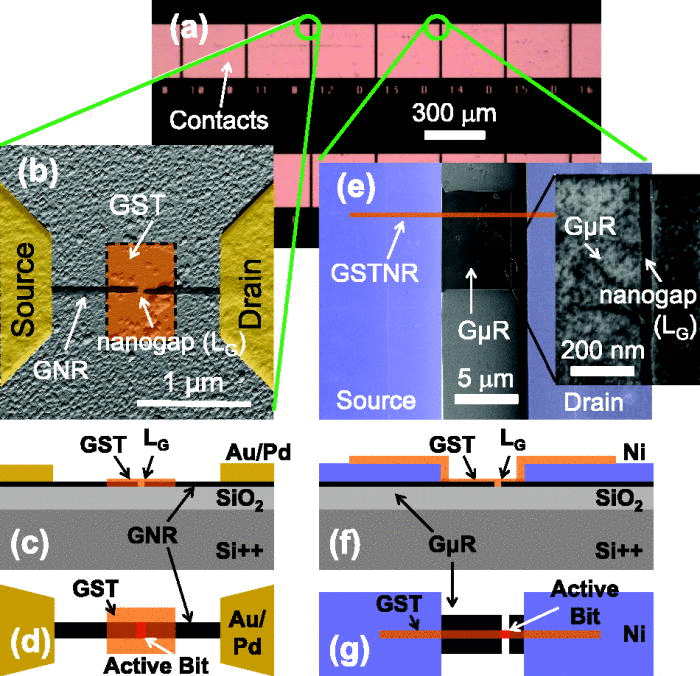
Abstract: “Phase change memory (PCM) devices are known to reduce in power consumption as the bit volume and contact area of their electrodes are scaled down. Here, we demonstrate two types of low-power PCM devices with lateral graphene ribbon electrodes: one in which the graphene is patterned into narrow nanoribbons and the other where the phase change material is patterned into nanoribbons. The sharp graphene “edge” contacts enable switching with threshold voltages as low as ∼3 V, low programming currents (<1 μA SET and <10 μA RESET) and OFF/ON resistance ratios >100. Large-scale fabrication with graphene grown by chemical vapor deposition also enables the study of heterogeneous integration and that of variability for such nanomaterials and devices”


 Subscribe to our free daily newsletter

