


Spectromicroscopic Insights for Rational Design of Redox-Based Memristive Devices
Novel concept for future non-volatile memory devices
By Francis Pelletier | October 26, 2015 at 2:48 pmNature Communications has published an article written by Christoph Baeumer, Peter Gruenberg Institute, Forschungszentrum Juelich GmbH and JARA-FIT, 52425 Juelich, Germany, Peter Gruenberg Institute, Forschungszentrum Juelich GmbH and JARA-FIT, 52425 Juelich, Germany, Christoph Schmitz, Peter Gruenberg Institute, Forschungszentrum Juelich GmbH and JARA-FIT, 52425 Juelich, Germany, Amr H. H. Ramadan, Institute of Physical Chemistry, RWTH Aachen University and JARA-FIT, 52056 Aachen, Germany, Hongchu Du, Peter Gruenberg Institute, Forschungszentrum Juelich GmbH and JARA-FIT, 52425 Juelich, Germany, and Ernst Ruska-Centre, Forschungszentrum Juelich GmbH and RWTH Aachen University, 52425 Juelich, Germany, Katharina Skaja, Vitaliy Feyer, Philipp Müller, Benedikt Arndt, Peter Gruenberg Institute, Forschungszentrum Juelich GmbH and JARA-FIT, 52425 Juelich, Germany, Chun-Lin Jia, Peter Gruenberg Institute, Forschungszentrum Juelich GmbH and JARA-FIT, 52425 Juelich, Germany, and Ernst Ruska-Centre, Forschungszentrum Juelich GmbH and RWTH Aachen University, 52425 Juelich, Germany, Joachim Mayer, Peter Gruenberg Institute, Forschungszentrum Juelich GmbH and JARA-FIT, 52425 Juelich, Germany, and Ernst Ruska-Centre, Forschungszentrum Juelich GmbH and RWTH Aachen University, 52425 Juelich, Germany, Roger A. De Souza, Institute of Physical Chemistry, RWTH Aachen University and JARA-FIT, 52056 Aachen, Germany, Claus Michael Schneider, Peter Gruenberg Institute, Forschungszentrum Juelich GmbH and JARA-FIT, 52425 Juelich, Germany, and Rainer Waser, Peter Gruenberg Institute, Forschungszentrum Juelich GmbH and JARA-FIT, 52425 Juelich, Germany, and Institute of Materials in Electrical Engineering and Information Technology II, RWTH Aachen University, 52056 Aachen, Germany, and Regina Dittmann, Peter Gruenberg Institute, Forschungszentrum Juelich GmbH and JARA-FIT, 52425 Juelich, Germany.
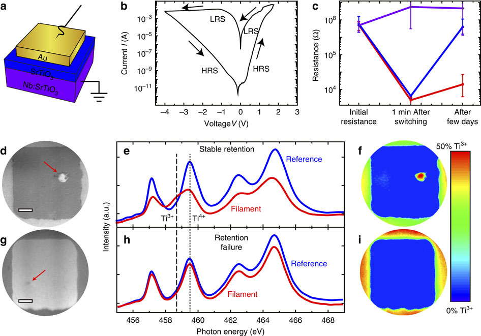
(a) Device schematic. (b) Representative I–V curve. (c) Retention behaviour of different devices on the same chip. Devices RESET into the HRS remain at a constant resistance over several days (violet curve). Devices that were SET into the LRS show two classes of retention behaviour: stable retention and retention failure (red and blue curves, respectively). For each class of retention behaviour, the resistance was averaged for five representative devices. Error bars indicate the minimum and maximum values obtained for each resistance state. (d) XPEEM image of a device with a stable retention recorded with a photon energy of 458.5 eV. Filament indicated by a red arrow. Scale bar, 2 μm. (e) Ti L-edge spectra extracted from the XPEEM image stack for a region inside the bright filament discernable in d (red line) and for the surrounding device area (blue line). The dotted line and the dashed line denote the eg level of the Ti L3 edge in Ti4+ and Ti3+ configuration, respectively. (f) False colour map of the Ti3+ contribution for the device in d. Only within the suspected switching filament, there is a significant spectral contribution of Ti3+. The enhanced contrast surrounding the active device is caused by the reactive ion beam etching involved in the electrode structuring and is not associated with the device conductance. (g) XPEEM image of a device with retention failure recorded with a photon energy of 459.5 eV. (h) Ti L-edge spectra extracted from the XPEEM image stack for a region inside the suspected switching filament discernable in g (red line) and for the surrounding device area (blue line). (i) False colour map of the Ti3+ spectral contribution for the device in g. No Ti3+ contribution is discernible for the entire device area.
Abstract : “The demand for highly scalable, low-power devices for data storage and logic operations is strongly stimulating research into resistive switching as a novel concept for future non-volatile memory devices. To meet technological requirements, it is imperative to have a set of material design rules based on fundamental material physics, but deriving such rules is proving challenging. Here, we elucidate both switching mechanism and failure mechanism in the valence-change model material SrTiO3, and on this basis we derive a design rule for failure-resistant devices. Spectromicroscopy reveals that the resistance change during device operation and failure is indeed caused by nanoscale oxygen migration resulting in localized valence changes between Ti4+ and Ti3+. While fast reoxidation typically results in retention failure in SrTiO3, local phase separation within the switching filament stabilizes the retention. Mimicking this phase separation by intentionally introducing retention-stabilization layers with slow oxygen transport improves retention times considerably.“


 Subscribe to our free daily newsletter

