R&D Light-Based Memory Chip Stores Data Permanently
Materials used in CDs and DVDs, could help improve speed of computing
This is a Press Release edited by StorageNewsletter.com on October 16, 2015 at 2:16 pmThe world’s first entirely light-based memory chip to store data permanently has been developed by material scientists at Oxford University in collaboration with scientists at Karlsruhe, Munster and Exeter.
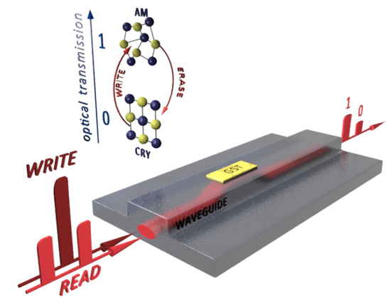
A schematic of the device, showing its structure
and the propagation of light through it.
(Credit: Image courtesy of University of Oxford)
The device, which makes use of materials used in CDs and DVDs, could help dramatically improve the speed of modern computing.
Today’s computers are held back by the relatively slow transmission of electronic data between the processor and the memory. “There’s no point using faster processors if the limiting factor is the shuttling of information to-and-from the memory — the so-called von-Neumann bottleneck,'” explains Professor Harish Bhaskaran, who led the research. “But we think using light can significantly speed this up.”
Simply bridging the processor-memory gap with photons isn’t efficient, though, because of the need to convert them back into electronic signals at each end. Instead, memory and processing capabilities would need be light-based too. Researchers have tried to create this kind of photonic memory before, but the results have always been volatile, requiring power in order to store data. For many applications — such as computer disk drives — it’s essential to be able to store data indefinitely, with or without power.
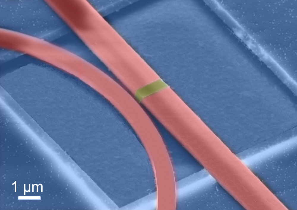
A scanning electron microscope image of the device.
The GST phase-change material, highlighted in yellow,
sits on top of the silicon nitride waveguide, highlighted in red.
Now, an international team of researchers including researchers from Oxford University’s Department of Materials has produced the world’s first all-photonic nonvolatile memory chip. The device uses the phase-change material Ge2Sb2Te5 (GST) – the same as that used in rewritable CDs and DVDs – to store data. This material can be made to assume an amorphous state, like glass, or a crystalline state, like a metal, by using either electrical or optical pulses. In a paper published in Nature Photonics (see below), the researchers describe the device they’ve created, which uses a small section of GST on top of a silicon nitride ridge, known as a waveguide, to carry light.
The team has shown that intense pulses of light sent through the waveguide can carefully change the state of the GST. An intense pulse causes it to momentarily melt and quickly cool, causing it to assume an amorphous structure; a slightly less-intense pulse can put it into an crystalline state.
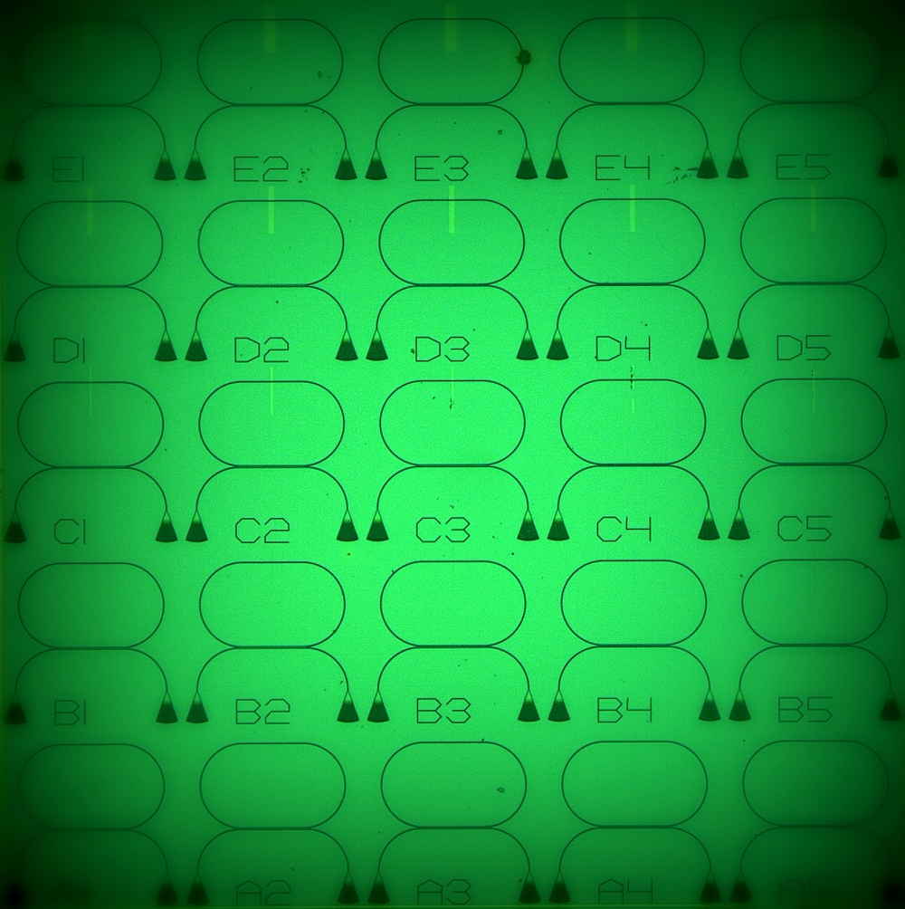
An optical microscope image of a chip containing
several memory elements on a ring resonator architecture.
Later, when light with much lower intensity is sent through the waveguide, the difference in the state of the GST affects how much light is transmitted. The team can measure that difference to identify its state — and in turn read off the presence of information in the device as a 1 or 0. “This is the first ever truly non-volatile integrated optical memory device to be created,” explains Clarendon Scholar and DPhil student Carlos Ríos, one of the two lead authors of the paper. “And we’ve achieved it using established materials that are known for their long-term data retention — GST remains in the state that it’s placed in for decades.“
By sending different wavelengths of light through the waveguide at the same time — a technique referred to as wavelength multiplexing — the team also showed that they could use a single pulse to write and read to the memory at the same time. “In theory, that means we could read and write to thousands of bits at once, providing virtually unlimited bandwidth,” explains Professor Wolfram Pernice of the University of Munster.
The researchers have also found that different intensities of strong pulses can accurately and repeatedly create different mixtures of amorphous and crystalline structure within the GST. When lower intensity pulses were sent through the waveguide to read the contents of the device, they were also able to detect the subtle differences in transmitted light, allowing them to reliably write and read off eight different levels of state composition — from entirely crystalline to completely amorphous. This multi-state capability could provide memory units with more than the usual binary information of 0 and 1, allowing a single bits of memory to store several states or even perform calculations themselves instead of at the processor.
“This is a completely new kind of functionality using proven existing materials,” explains Professor Bhaskaran. “These optical bits can be written with frequencies of up to one gigahertz and could provide huge bandwidths. This is the kind of ultra-fast data storage that modern computing needs.”
Now, the team is working on a number of projects that aim to make use of the new technology. They’re particularly interested in developing a new kind of electro-optical interconnect, which will allow the memory chips to directly interface with other components using light, rather than electrical signals.
The work was supported by the Engineering and Physical Sciences Research Council (EPSRC) and The John Fell Fund.
Article reference:
Nature Photonics has published the article written by Carlos Ríos, Department of Materials, University of Oxford, Parks Road, Oxford OX1 3PH, UK, Matthias Stegmaier, Institute of Nanotechnology, Karlsruhe Institute of Technology (KIT), Hermann-von-Helmholtz-Platz 1, Eggenstein-Leopoldshafen 76344, Germany, Peiman Hosseini, Department of Materials, University of Oxford, Parks Road, Oxford OX1 3PH, UK, Di Wang, Institute of Nanotechnology, Karlsruhe Institute of Technology (KIT), Hermann-von-Helmholtz-Platz 1, Eggenstein-Leopoldshafen 76344, Germany and Karlsruhe Nano Micro Facility (KNMF), Karlsruhe Institute of Technology (KIT), Hermann-von-Helmholtz-Platz 1, Eggenstein-Leopoldshafen 76344, Germany, Torsten Scherer, Institute of Nanotechnology, Karlsruhe Institute of Technology (KIT), Hermann-von-Helmholtz-Platz 1, Eggenstein-Leopoldshafen 76344, Germany and Karlsruhe Nano Micro Facility (KNMF), Karlsruhe Institute of Technology (KIT), Hermann-von-Helmholtz-Platz 1, Eggenstein-Leopoldshafen 76344, Germany, C. David Wright, Department of Engineering, University of Exeter, Exeter EX4 4QF, UK, Harish Bhaskaran, Department of Materials, University of Oxford, Parks Road, Oxford OX1 3PH, UK and Wolfram H. P. Pernice, Institute of Nanotechnology, Karlsruhe Institute of Technology (KIT), Hermann-von-Helmholtz-Platz 1, Eggenstein-Leopoldshafen 76344, Germany and Institute of Physics, University of Muenster, Muenster 48149, Germany and Institute of Physics, University of Muenster, Muenster 48149, Germany.
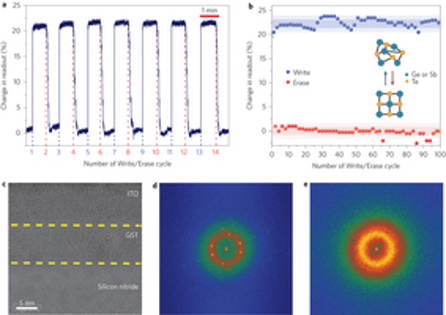
Demonstration of binary memory operation between the crystalline
(lower, Level 0) and amorphous (upper, Level 1)
state of a 5 µm GST device with a total change in readout transmission of 21%.
Abstract: “Implementing on-chip non-volatile photonic memories has been a long-term, yet elusive goal. Photonic data storage would dramatically improve performance in existing computing architectures by reducing the latencies associated with electrical memories and potentially eliminating optoelectronic conversions. Furthermore, multi-level photonic memories with random access would allow for leveraging even greater computational capability.. However, photonic memories have thus far been volatile. Here, we demonstrate a robust, non-volatile, all-photonic memory based on phase-change materials. By using optical near-field effects, we realize bit storage of up to eight levels in a single device that readily switches between intermediate states. Our on-chip memory cells feature single-shot readout and switching energies as low as 13.4 pJ at speeds approaching 1 GHz. We show that individual memory elements can be addressed using a wavelength multiplexing scheme. Our multi-level, multi-bit devices provide a pathway towards eliminating the von Neumann bottleneck and portend a new paradigm in all-photonic memory and non-conventional computing.”


 Subscribe to our free daily newsletter

