









Intel and Micron in 20nm MLC Flash Technology
8GB on 118mm²
This is a Press Release edited by StorageNewsletter.com on April 15, 2011 at 3:08 pmIntel Corporation and Micron Technology Inc. introduced a 20-nanometer (nm) process technology for manufacturing NAND flash memory.
The new 20nm process produces an 8-gigabyte (GB) multi-level cell (MLC)
NAND flash device, providing a high-capacity, small form factor storage
option for saving music, video, books and other data on smartphones,
tablets and computing solutions such as solid-state drives (SSDs).

New 64 Gigabit (Gb) NAND flash die from Intel Micron Flash
Technologies – Intel and Micron deliver the smallest NAND flash process
technology at 20nm. Shown is a 64Gb, or 8 Gigabyte (GB), die measuring
just 118mm². The 64Gb Multi-Level Cell (MLC) NAND device provides high
capacity for smartphones, tablets, SSDs and more.
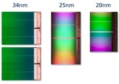
Comparison of two 32Gb 34nm die versus one 64Gb on 25nm and 20nm
process from IMFT – This photo shows a comparison of two 32 Gigabit
(Gb) Intel Micron Flash Technologies (IMFT) 34nm die versus one 64Gb, or
8 Gigabyte (GB), die on 25nm and new 20nm processes. Shrinking NAND
lithography is the most cost-effective method for increasing fab output
and reducing die cost. Shrinking from 25nm to 20nm process will provide
an approximately 50 percent more gigabyte capacity from IMFT factories
when compared to current technology. The new 20nm process maintains
similar performance and endurance as the previous generation 25nm NAND
technology.
The growth in data storage combined with feature enhancements for
tablets and smartphones is creating new demands for NAND flash
technology, especially greater capacity in smaller designs. The new 20nm
8GB device measures 118mm² and enables a 30 to 40 percent reduction in board space (depending on package type) compared to the companies’ existing 25nm
8GB NAND device. A reduction in the flash storage layout provides
greater system level efficiency as it enables tablet and smartphone
manufacturers to use the extra space for end-product improvements such
as a bigger battery, larger screen or adding another chip to handle new
features.
It is manufactured by IM Flash Technologies (IMFT), Intel and Micron’s
NAND flash joint venture. Shrinking NAND lithography to this technology
node is a cost-effective method for increasing fab output, as it
provides approximately 50 percent more gigabyte capacity from these
factories when compared to current technology. The new 20nm process
maintains similar performance and endurance as the previous generation 25nm NAND technology.
"Close customer collaboration is one of Micron’s core values and through
these efforts we are constantly uncovering compelling end-product
design opportunities for NAND flash storage," said Glen Hawk, vice
president of Micron’s NAND Solutions Group. "Our innovation and growth
opportunities continue with the 20nm NAND process, enabling Micron to
deliver cost-effective, value-added solid-state storage solutions for
our customers."
"Our goal is to enable instant, affordable access to the world’s
information," said Tom Rampone, vice president and general manager,
Intel Non-Volatile Memory Solutions Group. "Industry-leading NAND gives
Intel the ability to provide the highest quality and most cost-effective
solutions to our customers, generation after generation. The
Intel-Micron joint venture is a model for the manufacturing industry as
we continue to lead the industry in process technology and make quick
transitions of our entire fab network to smaller and smaller
lithographies."
The 20nm, 8GB device is sampling now and expected to enter mass
production in the second half of 2011. At that time, Intel and Micron
also expect to unveil samples of a 16GB device, creating up to 128GBs of
capacity in a single solid-state storage solution that is smaller than a
U.S. postage stamp.
Comments
Flash technology is improving fast, faster than HDD areal density.
Intel Micron Flash Technologies, the Intel Micron JV, started production with a 50nm process in 2006, followed by a 34nm process in 2008. It introduces 25nm NAND chips in February 2010 available since 2Q10.
In a little more than one year, it's a 30% to 40% increase in flash density to get 128GB in a solution "smaller than a U.S. postage stamp".
Here is a chart from Wikipedia showing
the evolution of flash chips by four manufacturers
from 2007 to now:









 Subscribe to our free daily newsletter


