









Intel and Micron in 25nm NAND Technology
For 8GB in a single chip, to be produced in 2Q10
This is a Press Release edited by StorageNewsletter.com on February 2, 2010 at 3:17 pmIntel Corporation and Micron Technology, Inc. announced the world’s first 25-nanometer (nm) NAND technology, which provides a more cost-effective path for increasing storage capacity in such popular consumer gadgets as smartphones, personal music and media players (PMPs), as well as the new high-performance class of solid-state drives (SSDs).
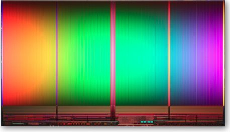
NAND flash memory stores data and other media contained in consumer electronics products, retaining information even when the power is turned off. The drive toward smaller NAND processes enables the continued development and introduction of new uses for the technology. Not only is the 25nm process the smallest NAND technology, it is also the smallest semiconductor technology in the world, a technological accomplishment that continues the advancement of more music, video, and other data in today’s consumer electronics and computing applications.
Manufactured by IM Flash Technologies (IMFT), Intel and Micron’s NAND flash joint venture, the 25nm process produces 8 gigabytes (GB) of storage in a single NAND device, creating a high-capacity storage solution for today’s tiny consumer gadgets. It measures just 167mm² – small enough to fit through the hole in the middle of a compact disc (CD), yet packs more than 10 times the data capacity of that CD (a standard CD holds 700 megabytes of data).
With a committed focus and investment in NAND research and development, Intel and Micron have doubled NAND density roughly every 18 months, which leads to smaller, more cost-efficient and higher capacity products. Intel and Micron formed IMFT in 2006, starting production with a 50nm process, followed by a 34nm process in 2008. With today’s 25nm process, the companies are extending their process and fabrication leadership further with the introduction of the smallest semiconductor lithography available in the industry.
"To lead the entire semiconductor industry with the most advanced process technology is a phenomenal feat for Intel and Micron, and we look forward to further pushing the scaling limits," said Brian Shirley, vice president of Micron’s memory group. "This production technology will enable significant benefits to our customers through higher density media solutions."
"Through our continued investment in IMFT, we’re delivering leadership technology and manufacturing that enable the most cost-effective and reliable NAND memory," said Tom Rampone, vice president and general manager, Intel NAND Solutions Group. "This will help speed the adoption of solid-state drive solutions for computing."
The 25nm, 8GB device is sampling now and is expected to enter mass production in the second quarter of 2010. For consumer electronics manufacturers, the device provides the highest-density in a single 2 bits-per-cell multi-level cell (MLC) die that will fit an industry-standard, thin small-outline package (TSOP). Multiple 8GB devices can be stacked in a package to increase storage capacity. The new 25nm 8GB device reduces chip count by 50 percent compared to previous process generations, allowing for smaller, yet higher density designs and greater cost efficiencies. For example, a 256GB solid-state drive (SSD) can now be enabled with just 32 of these devices (versus 64 previously), a 32GB smartphone needs just four, and a 16GB flash card requires only two.
Comments
Here are commentd by Jim Handy, Objective Analysis:
In an effort to remain a full process node ahead of other NAND flash manufacturers, Intel and Micron today announced that the companies' IMFT joint venture has now introduced a 25nm 64Gb MLC NAND chip. This translates to 8 gigabytes on a single chip. With a die size of 167mm² the device can fit into a standard TSOP package.
The announcement follows the companies' May 2008 introduction of a 34nm 32Gb NAND.
At a die size of 167mm², a 300mm fab should be able to manufacture just over 400 dice per wafer. This gives a manufacturing cost of about $4.00 per chip, or $0.50/GB. Compare this to a more common 45nm MLC NAND on a 300mm line which should cost about $1.75/GB. Since the price of NAND flash has been hovering around $2.00/GB for the past year, and seems poised to continue at that price through 2010, the 25nm process will give the companies a significant margin boost over their current 34nm chip whose cost we estimate at $1.00/GB.
The companies made it very clear that they do not plan to drive prices down to follow cost. Instead, we can expect for Micron and Intel to continue to charge market prices and simply pocket larger margins than can their competition.
Both companies are currently sampling to select customers and controller makers. Both also remarked that this was one further step that would help bring SSDs into the mainstream.
The companies point out that they entered the market with a 72nm technology in 2006, which they believe was about 2 years behind their competition, but caught up and surpassed these competitors by as much as a year with the 34nm part, and are maintaining this leadership by migrating to 25nm at the same time that some of their competitors are ramping their 30nm-generation processes.
Not only will this new process allow Micron and Intel to profit more than their competition, but it also allows them to squeeze more gigabyte production out of their Lehi and Manassas lines before having to equip their new fab in Singapore.








 Subscribe to our free daily newsletter


