


… Toshiba Develops First 256Gb, 48-Layer BiCS FLASH …
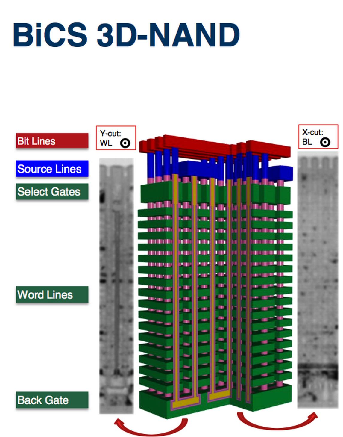
3D stacked cell structure flash memory
This is a Press Release edited by StorageNewsletter.com on August 5, 2015 at 3:01 pmToshiba America Electronic Components, Inc. (TAEC) unveiled the new generation of BiCS FLASH, a three-dimensional (3D) stacked cell structure flash memory (1).
The new device is the first (2) 256Gb (4) (32GB) 48-layer BiCS FLASH device and also deploys 3-bit-per-cell TLC (triple-level cell) technology.
Sample shipments will start in September.
BiCS FLASH is based on a 48-layer stacking process that surpasses the capacity of mainstream two dimensional NAND flash memory, while enhancing write/erase reliability endurance and boosting write speeds. The new 256Gb device is suited for diverse applications, including consumer SSDs, smartphones, tablets, memory cards, and enterprise SSDs for data centers.
Since announcing the prototype BiCS FLASH technology in June 2007, Toshiba has continued development towards optimization for mass production. To meet further growth in the flash memory market in 2016 and beyond, Toshiba is proactively promoting migration to BiCS FLASH by rolling out a product portfolio that emphasizes large capacity applications, such as SSDs.
“From day one, Toshiba’s strategy has been to extend our floating gate technology, which features the world’s smallest 15nm 128Gb die (3) ,” noted Scott Nelson, SVP of TAEC’s memory business unit. “Our announcement of BiCS FLASH, the industry’s first 48-layer 3D technology, is very significant in that we are enabling a competitive, smooth migration to 3D flash memory – to support the storage market’s demand for ever-increasing densities.”
Toshiba has a long-standing commitment to flash memory, and is currently readying for mass production of BiCS FLASH in the new Fab2 at Yokkaichi Operations, its production site for NAND flash memories. Fab2 will be completed in the first half of 2016.
(1) A structure stacking Flash memory cells vertically on a silicon substrate to realize significant density improvements over planar NAND Flash memory, where cells are formed on the silicon substrate.
(2) As of August 4, 2015. Toshiba survey.
(3) As of August 4, 2015. Toshiba survey.
(4) Product density is identified based on the density of memory chip(s) within the Product, not the amount of memory capacity available for data storage by the end user. Consumer-usable capacity will be less due to overhead data areas, formatting, bad blocks, and other constraints, and may also vary based on the host device and application.


 Subscribe to our free daily newsletter


