


More on Future of Toshiba 3D NAND Flash Memory
BiCS will reach for 100 layers and beyond.
This is a Press Release edited by StorageNewsletter.com on August 11, 2016 at 6:18 pmBack in June 2007, Toshiba Corp. unveiled the prototype of a new type of NAND flash architecture, one with a three dimensional memory cell array structure that enhances cell density and data capacity without relying on advances in process technology.
Not surprisingly, it did not cause much of a stir. Although NAND flash was already making a difference in MP3 players, digital cameras and memory cards, the big breakthrough of smartphones was yet to come.
But even then, in those early days, Toshiba was looking far ahead into the future of flash memory, toward the successor of the still emerging technology.
In 1965, Gordon Moore, of Intel fame, observed that the number of transistors on an integrated circuit was doubling every year, and would continue to do so for at least a decade. Revisiting what had become known as Moore’s Law in 1975, he revised the period to two years, and the time span to indefinitely.
Of course, indefinitely is not forever …
Hitting the wall
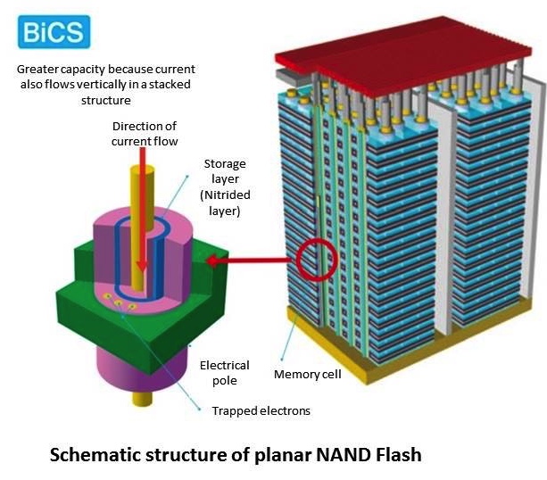
In conventional NAND flash, memory cells that store data are formed as a single layer on a silicon substrate, a planar architecture. Each memory cell has a floating gate that traps electrons, and initially a single cell held-or didn’t hold-a single bit of data, depending on the presence or absence of electrons. Advances in controlling the number of electrons in the gate, to create states where there are more or fewer electrons, have made it possible to increase the number of bits stored in each cell, a process known as MLC technology. So until today, progress in NAND flash has been based on increasing the number of cells on a chip and the number of bits each cell can store. And that progress has been formidable.
NAND flash is a marvel of manufacturing. The fabs at Toshiba’s Yokkaichi Operations churn out chip after chip made with process technology that forms circuits as narrow as 15-nanometers wide; that’s 0.000000015 of a meter, so fine that individual lines are invisible to the human eye.
The problem is that 15-nanometers is way out there at the far end of Moore’s Law, just short of the point where, with current technologies, packing more cells onto a chip will generate too much heat and noise, and see electrons bleed between circuit lines. Perhaps a few nm more can be wrung out of current approaches, but beyond that, the game is over. It’s a bit like the marathon. The world record has been chipped away at for years, but human biomechanics can only achieve so much, and there’s a point where further improvement becomes impossible.
Creating a new architecture
Property developers respond to increasing population density by building up or out. With ICs, out is not an option. The whole point of semiconductors is small size, dense packing, miniaturization. That’s why Toshiba’s engineers have spent the last decade refining a new three-dimensional flash architecture that builds up, layer upon layer, from a single substrate, while retaining the small die size and, most important, the low profile of current chips.
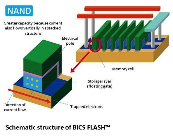
The final target has always been twofold: to stack layers of memory cells on a silicon base that is not much bigger than a current NAND flash chip; and to achieve densities that surpass current chips. The result, BiCS FLASH, is the much developed, much improved successor to the 3D chip announced back in 2007.
Toshiba’s memory engineers have painstakingly pushed the process forward, developing an optimized cell structure and a process that secures reliable data write and erase endurance, plus the faster write speeds for the most demanding applications. Stacking also allows the formation of larger cells than a planar structure, another performance-enhancing advantage.
Moving forward and up
As work on BiCS FLASH has advanced, so has Toshiba’s strategy. In May 2014, the company announced that it would raze fab 2 at its Yokkaichi Operations in central Japan, and that a new fab 2, dedicated to BiCS FLASH would rise on the same site. And it has. In mid-July this year, the new fab was officially opened, and is now operational.
In March 2015, as the frame for new fab 2 took shape and form, Toshiba announced a 48-layer BiCS FLASH, a 128Gb device robust enough for enterprise SSD, the most demanding application of all. Only a few months later, in August, the company announced a 48-layer, 256Gb device able to store three bits of data in a cell (TLC technology).
Now, Toshiba has moved to the next level.
On July 27, it became the first company to announce sample shipments of a 64-layer 3D flash memory, with a 256Gb capacity and TLC technology. This successor to the 48-layer device has a 40% larger capacity per chip size, a lower production cost per bit, and also increases the memory capacity that can be manufactured from a single silicon wafer. Like its predecessor, the 64-layer BiCS FLASH can meet demanding performance specs, and its long list of potential applications includes enterprise and consumer SSD, smartphones, tablets and memory cards.
Over the last year, Toshiba has seen the fruition of a long and rigorous research program, and established a new direction for NAND flash and the semiconductor industry. Now, the company’s focus is on achieving the potential of BiCS FLASH. In fact, the press release announced the 64-layer device also included a promise of things to come: “the next milestone on the development roadmap is a 512Gb device, also with 64 layers.”
With BiCS FLASH now a tried, tested and proven technology, the company will continue to build up, to reach for 100 layers and beyond.


 Subscribe to our free daily newsletter

