


Charge-Trap Non-Volatile Memories Fabricated by Laser-Enabled Low-Thermal Budget Processe
Including laser-crystallization of poly-Si thin film, chemical vapor deposition deposition of stacked memory layer, and far-infrared-laser dopant activation.
This is a Press Release edited by StorageNewsletter.com on November 12, 2015 at 2:45 pmApplied Physics Letters has published an article written by Wen-Hsien Huang, Department of Materials Science and Engineering, National Chiao-Tung University, Hsinchu 30010 Taiwan, and National Nano Device Laboratories, No. 26, Prosperity Road 1, Hsinchu 30078, Taiwan, Jia-Min Shieh, National Nano Device Laboratories, No. 26, Prosperity Road 1, Hsinchu 30078, Taiwan, Fu-Ming Pan, Department of Materials Science and Engineering, National Chiao-Tung University, Hsinchu 30010 Taiwan , Chih-Chao Yang,National Nano Device Laboratories, No. 26, Prosperity Road 1, Hsinchu 30078, Taiwan , Chang-Hong Shen, Hsing-Hsiang Wang, Tung-Ying Hsieh,National Nano Device Laboratories, No. 26, Prosperity Road 1, Hsinchu 30078, Taiwan, Ssu-Yu Wu, and Meng-Chyi Wu, Department of Electrical Engineering, National Tsing Hua University, Sec. 2, Kuang-Fu Road, Hsinchu 30013, Taiwan.
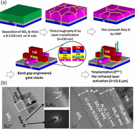
(a) The schematic illustration of the fabrication processes of MONAOS NVM with a thin/smooth poly-Si channel layer, a band-gap engineered memory stack at the TiN gate, and far-infrared laser dopant activation; (b) the cross-sectional TEM image of MONAOS NVM (W/L = 70/70 nm) with the preferential orientation, SADP of the poly-Si channel layer, and the enlarged image of the stacked memory layers.
Abstract : “We fabricated charge-trap non-volatile memories (NVMs) using low thermal budget processes, including laser-crystallization of poly-Si thin film, chemical vapor deposition deposition of a stacked memory layer, and far-infrared-laser dopant activation. The thin poly-Si channel has a low defect-density at the interface with the bulk, resulting in a steep subthreshold swing for the NVM transistors. The introduction of the stacked SiO2/AlOxNy tunnel layer and the SiNx charge-trap layer with a gradient bandgap leads to reliable retention and endurance at low voltage for the NVMs. The low thermal budget processes are desirable for the integration of the nano-scaled NVMs into system on panels.“


 Subscribe to our free daily newsletter
