


Toshiba Yokkaichi Operations
Currently covering 50 flavors of NAND flash
This is a Press Release edited by StorageNewsletter.com on August 12, 2016 at 6:22 pmSeen from the road, the buildings of Toshiba Corp.‘s Yokkaichi operations loom large and almost featureless.
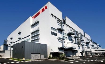
With few windows, their gray-white of their walls relieved only by the red of Toshiba’s logo, they are uncommunicative, almost mysterious. They also form the world’s largest single complex dedicated to manufacturing NAND flash memory, and one of them, New Fab 2, is also the newest.
X marks the spot. A birds-eye view of New Fab 2 in Yokkaichi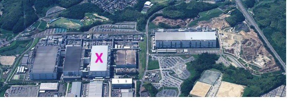
NAND flash, a semiconductor memory that retains data even without a power supply, was invented by Toshiba in the 1980s. Its advantages of long-term resilience and robustness from having no moving parts have, over the years, combined with technology refinements, capacity increases and falling prices to make NAND a winner in storage. Today it is the enabling technology for everything from the smartphone in nearly everybody’s pocket to the vast server farms that sustain on-line services.
A lot of the interest in NAND is about the process technologies used in its manufacture. The main questions are how many more transistors can be squeezed onto a chip, and how fine can the manufacturing process get? As Toshiba works ceaselessly to shrink it process to the lowest level possible, those are also questions Toshiba asks itself. But, it also asks other questions, which can be boiled down to one simple question: How do we make Yokkaichi not only the biggest NAND manufacturing facility, but also the best?
All manufacturing facilities want to optimize throughput and maximize yield. The first concentrates on the flow through production processes, to remove any bottlenecks or black spots, the second on the output of usable product.
Masanori Morikawa, former senior manager of the manufacturing engineering dept. at Yokkaichi operations, neatly sums up the facility’s goal: “We want to eliminate everything that is muda,” he says: using a word that nicely translates as futile or useless. His ideal is a production plant where everything runs perfectly. Of course, that’s impossible in practice-but that’s no reason for not making the effort.
Yokkaichi’s key performance indicator, its basic metric for working toward muda-free operation, is the cost of 1GB of production. The endless challenge is to constantly drive that cost as low as possible.
Bring on big data and AI
Production in Yokkaichi’s fabs currently covers 50 flavors of NAND flash. They go through 20,000 processes, carried out on 200 different kinds of manufacturing equipment, and there are 4,000 pieces of equipment in all. Every process is monitored, and the data generated is used to squeeze out incremental improvements and to troubleshoot problems as soon as possible. While that’s all simple enough to write, on the production line it’s a ceaseless and intensive process. Every single day sees the generation of 1.6 billion separate data points, a rate of nearly 70 million pieces of data an hour, over 1.1 million a minute. It’s an avalanche of information that could overwhelm an army of engineers, and the point where AI and big data analytics step in.
Clean room in New Fab 2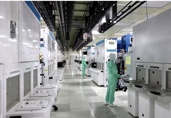
One way computers help is in spotting flaws in circuits by visual inspection of wafers. Until now, that has been done by a technician examining an enlarged image of the wafer surface, scanning it for blemishes and irregularities. Today, technicians at Yokkaichi are teaching computers to use deep learning to quickly and efficiently scan wafers, to look for loops, scratches, breaks in the circuit pattern and other problems, all without the human risk of growing tired or being distracted.
For Yokkaichi’s engineers however, finding flaws is only the beginning. They want to know when and how they happened, and what to do to avoid any recurrence. Towards that, the operation of every piece of equipment is monitored, through all sub-routines, to help identify and eliminate any sources of muda. Even two apparently identical pieces of equipment from the same manufacturer can turn out to have different performance profiles, and the data provides the key to understanding this.
Another area where big data helps out is logistics and the movement of individual wafers. At Yokkaichi, this is all automated. From the time a wafer leaves the warehouse to the moment when it is ready for shipping, it is moved from point to point on an overhead transportation system. Each vehicle in the system is monitored by sensors that show where it is, and, if it is not moving, how long it has been waiting at that point, and why it is waiting.
Yokkaichi’s overhead wafer transportation system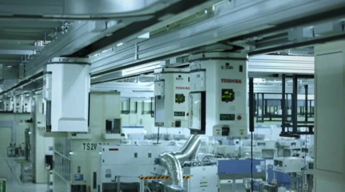
Better understanding, better manufacturing
All this unstructured data is fed into a large array of computers built as a Hadoop cluster; a distributed, scalable configuration with the capacity and power required to store and analyze data from Yokkaichi’s billions of data transactions.
The results guide engineers in areas as diverse as servie and maintenance, line configuration nd flow, so as to secure the highest throughput, maximized equipment uptime, and highest yield. It can tell them when to send a wafer to which machine, when that machine should be taken offline, and where the addition of a machine will enhance the flow. To take one example, it quickly showed that storing all wafers in a single location prior to processing was a bottleneck in itself, a mistake quickly rectified.
The biggest test of the accumulated know-how that Toshiba applies at Yokkaichi is now being faced. At the start of this article, we mentioned New Fab 2, the newest facility on the Yokkaichi site. It opened on July 15 this year, and will focus on the manufacture of 3D BiCS FLASH, a new approach to NAND that uses a stacked structure to build layers of memory cells on top of another.* In this new fab, producing a cutting-edge new product, Toshiba will seek to make the dream of muda-free manufacturing a reality.


 Subscribe to our free daily newsletter

