FMS: Samsung Starts Production of 250GB SATA SSD With Sixth-Gen 256Gb 3-bit V-NAND
Plans to offer 512Gb 3-bit V-NAND SSD and eUFS, below 450μs for write and 45μs for read operations.
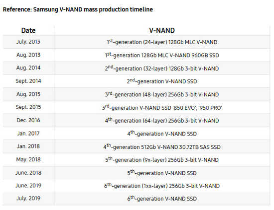
This is a Press Release edited by StorageNewsletter.com on August 12, 2019 at 2:40 pmSamsung Electronics Co., Ltd. began mass producing 250GB SATA SSD that integrates the company’s sixth-gen (1xx-layer) 256Gb 3-bit V-NAND for gPC OEMs.

By launching a new gen of V-NAND in just 13 months, the company has reduced the mass production cycle by 4 months while securing the industry’s performance, power efficiency and manufacturing productivity.
“By bringing cutting-edge 3D memory technology to volume production, we are able to introduce timely memory lineups that raise the bar for speed and power efficiency,” said Kye Hyun Kyung, EVP, solution product and development, Samsung. “With faster development cycles for next-gen V-NAND products, we plan to rapidly expand the markets for our high-speed, high-capacity 512Gb V-NAND-based solutions.“
The single-stack 3D memory die with a 100+ layer design firm’s sixth-generation V-NAND features a fast data transfer rate, capitalizing on the company’s distinct manufacturing edge that is taking 3D memory to new heights.
Utilizing the company’s channel hole etching’ technology, the V-NAND adds around 40<ù more cells to the previous 9x-layer single-stack structure. This is achieved by building an electrically conductive mold stack comprised of 136 layers, then vertically piercing cylindrical holes from top to bottom, creating uniform 3D charge trap flash (CTF) cells.
As the mold stack in each cell area increases in height, NAND flash chips tend to become more vulnerable to errors and read latencies. To overcome such limitations, Samsung has incorporated a speed-optimized circuit design that allows it to achieve fast data transfer speed, at below 450μs for write operations and below 45μs for reads. Compared to the previous gen, this represents a more than 10% improvement in performance, while power consumption is reduced by more than 15%.
Thanks to this speed-optimized design, the company will be able to offer next-generation V-NAND solutions with over 300 layers simply by mounting three of the current stacks, without compromising chip performance or reliability.
In addition, the number of channel holes required to create a 256Gb chip density has decreased to 670 million holes from over 930 million with the previous gen, enabling reduced chip sizes and less process steps. This brings a more than 20% improvement in manufacturing productivity.
Leveraging the high-speed and low-power features, the firm plans to broaden the reach of its 3D V-NAND into areas like next-gen mobile devices and enterprise servers, and also into the automotive market where reliability is critical.
Following introduction of the 250GB SSD, the company plans to offer 512Gb three-bit V-NAND SSD and eUFS in 2H19. It also expects to expand production of higher-speed and capacity sixth-gen V-NAND solutions at its Pyeongtaek campus, Korea, starting next year.


 Subscribe to our free daily newsletter

