


R&D: IBM Researchers Demo Scalability of Spin Torque MRAM for Next Decade
Down to 11 nanometers
This is a Press Release edited by StorageNewsletter.com on July 19, 2016 at 3:09 pmThis article was published on IBM Research blog.
Researchers celebrate 20th anniversary of IBM’s invention of Spin Torque MRAM by demonstrating scalability for the next decade
“A new mechanism is proposed for exciting the magnetic state of a ferromagnet.“
 By Chris Sciacca, communications manager, EMEA, IBM Research
Twenty years ago these words were written by IBM scientist John Slonczewski in his now seminal paper “Current-driven excitation of magnetic multilayers” in the Journal of Magnetism and Magnetic Materials. And today they are helping scientists overcome several technical hurdles in the development of the memory that IBM’s Slonczewski invented: Spin Torque MRAM.
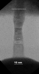
Transmission Electron Microscope (TEM) image of an 11nm junction
The timing for a new memory technology couldn’t be better as more demanding cognitive applications emerge, which require ingesting petabytes of structured and unstructured data for applications spanning the understanding of cancer metastasis, to the forecasting of natural disasters.
Understanding the memory hierarchy
Today, there are three main ways to store digital information, or bits, in the forms of 0’s and 1’s: HDDs, DRAM and flash memory.
HDDs, invented by IBM in the 1950s, continue to be attractive for PCs and data centers due to their low-cost. But these devices are intrinsically slower, require quite a bit of power, and due to their mechanical moving parts, are less reliable.
In 1967, IBM fellow Robert Dennard filed a patent for his world-changing invention known as DRAM. Decades later it remains a veritable workhorse, driving almost all computing devices today. Its main drawback is that it’s volatile, meaning when the device shuts off power, DRAM loses the data. This is particularly a problem for any number of applications, such as remote sensor devices with small batteries used for the IoT.
Today’s top non-volatile memory technology (retains data without the need for continued power) is flash, which can be found in devices ranging from USB sticks to the cloud. It is much faster at reading and writing data compared to HDDs, but is a laggard compared to DRAM. It also has an endurance problem, eventually breaking down after several thousand rewrite cycles.
For two decades, IBM scientists have been investigating several non-volatile memory devices including magneto-resistive random-access memory or MRAM, which uses the spin of an electron to store bits.
“We’ve been demonstrating IBM OpenPower systems’ value with non-volatile memory and believe non-volatile memory will be one of the biggest cost-performance levers for future datacenters,” said Bradley McCredie, IBM fellow and VP of Power Systems development.
Guohan Hu, manager of the MRAM materials and devices group
optimized perpendicular magnetic materials
to enable ultra-low write-error-rate.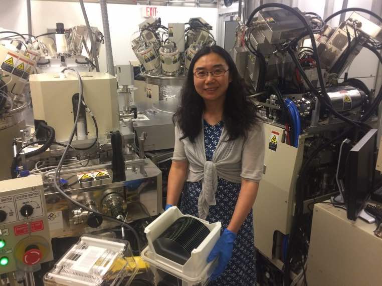
What is MRAM?
MRAM is based on a grid of cells with two ferromagnetic layers, separated by a thin insulating layer. When the two magnets are both pointing north, this corresponds to a ‘0’. If the second magnet points south, they store a ‘1’.
The first generation of MRAM, called field-switched MRAM, was written by applying large currents to generate magnetic fields to switch the second magnet between north and south.
However, Slonczewski saw a better way. When a current is passed through the cell, the electrons transfer their spin from one magnet to the other and thereby switch the second magnet from north to south, or vice versa, thus writing the cell
When introducing this invention in his 1996 paper, Slonczewski coined the term ‘spin transfer’ torque to describe this new switching mechanism. This new generation of MRAM is called Spin Transfer Torque MRAM (often shortened to Spin Torque MRAM or STT-MRAM).
IBM invents Spin Torque MRAM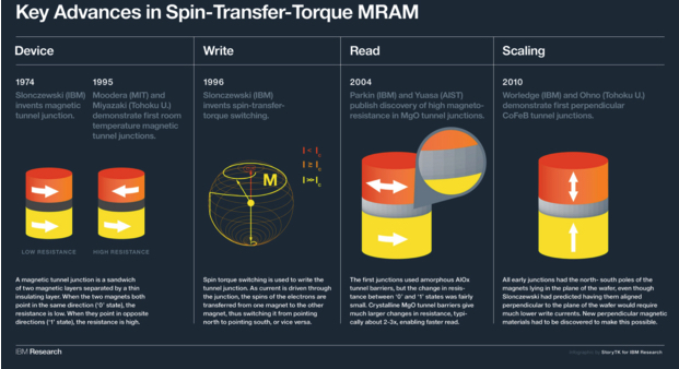
While first generation field-switched MRAM has been produced for years, technical challenges including lowering the write current prevented it from being scalable to high densities and thus wider adoption. Slonczewski’s invention opened up the possibility of using much smaller write currents, and hence much smaller write transistors, thus enabling much denser MRAM. However, to realize its potential, a breakthrough in materials would still be required.
Inspired by Slonczewski, scientists around the world, including teams at IBM and Samsung, continued to believe in the promise of MRAM because it offers several distinct advantages. MRAM is the only memory (or indeed emerging memory) that combines unlimited endurance (read and write cycles), with inherent non-volatility.
This combination makes MRAM an ideal technology for always-on devices such as IoT sensors, mobile devices and wearable electronics, offering more storage and longer battery life. In addition, since MRAM uses standard transistors, and is compact and robust, it’s more easily embedded on the same chip as logic and other functions, compared to flash memory. Therefore many semiconductor foundries are considering replacing embedded flash with embedded Spin Torque MRAM at the 28nm node and beyond.
“With these capabilities a single MRAM chip can replace a combination of SRAM and flash for many ultra-low power, medium performance mobile and Internet of Things applications. However, our long term goal remains to scale Spin Torque MRAM to be so dense and fast it can be used as a cache memory in IBM’s servers,” said Dr. Daniel Worledge, a scientist and MRAM team senior manager at IBM Research.
IBM scientist Janusz Nowak co-authored a paper
on scalling STT MRAM down to 11nm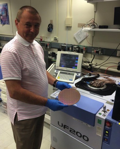
In 2011 Worledge and his colleagues published a paper which demonstrated a novel technique to produce MRAM with manufacturing line widths below 20nm. They called it perpendicular magnetic anisotropy (PMA). It was a critical discovery because it would enable Spin Torque MRAM to scale to much higher densities, thus fulfilling Slonczewski’s prediction in 1996. The trick was to develop magnetic materials that allowed the magnet to point perpendicular to the plane, instead of in the plane. While it was a notable achievement, Worledge and his colleagues knew they could scale even further, resulting in even denser MRAM to further bring costs down.
Worledge adds: “Unless we could increase the density and speed, we knew that use as a cache memory would never happen. So we went back to the drawing board to scale further.”
Reaching 11nm
Appearing in IEEE Magnetic Letters, Worledge and his IBM colleagues and partners at Samsung have published a paper Dependence of Voltage and Size on Write Error Rates in Spin-Transfer Torque Magnetic Random-Access Memory demonstrating switching MRAM cells for devices with diameters ranging from 50 down to 11nm in only 10 nanoseconds, using only 7.5 microamperes – a significant achievement.
“With PMA we are capable of delivering good STT-MRAM performance down to 7×10⁻¹⁰ write-error-rate with 10 nanosecond pulses using switching currents of only 7.5 microampere. This could never be done with in-plane magnetized devices – they just don’t scale. While more research needs to be done, this should give the industry the confidence it needs to move forward. The time for Spin Torque MRAM is now,” said Worledge.
“In the 20 years since these scientific discoveries at IBM Research and elsewhere, the phenomenon of spin transfer torque has inspired significant R&D effort. These have now led to an STT switched magnetic memory device of 11nm in size, back-end integrated onto CMOS circuits. This advance brings more possibilities to applications, and will accelerate the pace of innovation in the solid-state memory technology space,” said Jonathan Sun, a research staff member on Worledge’s team.
Spin Torque MRAM Symposium
On November 7, IBM is hosting a special 20th Anniversary Spin Torque MRAM Symposium at the Thomas J. Watson Research Center in Yorktown Heights, NY. The one day event will feature a series of talks including keynotes by Slonczewski and other scientists from around the world.


 Subscribe to our free daily newsletter
