


Integrated All-Photonic Non-Volatile Multi-Level Memory
Photonic storage would improve performance in existing computing architectures
This is a Press Release edited by StorageNewsletter.com on October 5, 2015 at 2:32 pmIntegrated all-photonic non-volatile multi-level memory
by Carlos Ríos, Matthias Stegmaier, Peiman Hosseini, Di Wang, Torsten Scherer, C. David Wright, Harish Bhaskaran & Wolfram H. P. Pernice
(Source: Nature Photonics (2015) doi:10.1038/nphoton.2015.182)
Implementing on-chip non-volatile photonic memories has been a long-term, yet elusive goal. Photonic data storage would dramatically improve performance in existing computing architectures1 by reducing the latencies associated with electrical memories and potentially eliminating optoelectronic conversions. Furthermore, multi-level photonic memories with random access would allow for leveraging even greater computational capability. However, photonic memories have thus far been volatile. Here, we demonstrate a robust, non-volatile, all-photonic memory based on phase-change materials. By using optical near-field effects, we realize bit storage of up to eight levels in a single device that readily switches between intermediate states. Our on-chip memory cells feature single-shot readout and switching energies as low as 13.4 pJ at speeds approaching 1GHz. We show that individual memory elements can be addressed using a wavelength multiplexing scheme. Our multi-level, multi-bit devices provide a pathway towards eliminating the von Neumann bottleneck and portend a new paradigm in all-photonic memory and non-conventional computing.
Figure 1: Operation principle of the all-optical on-chip memory device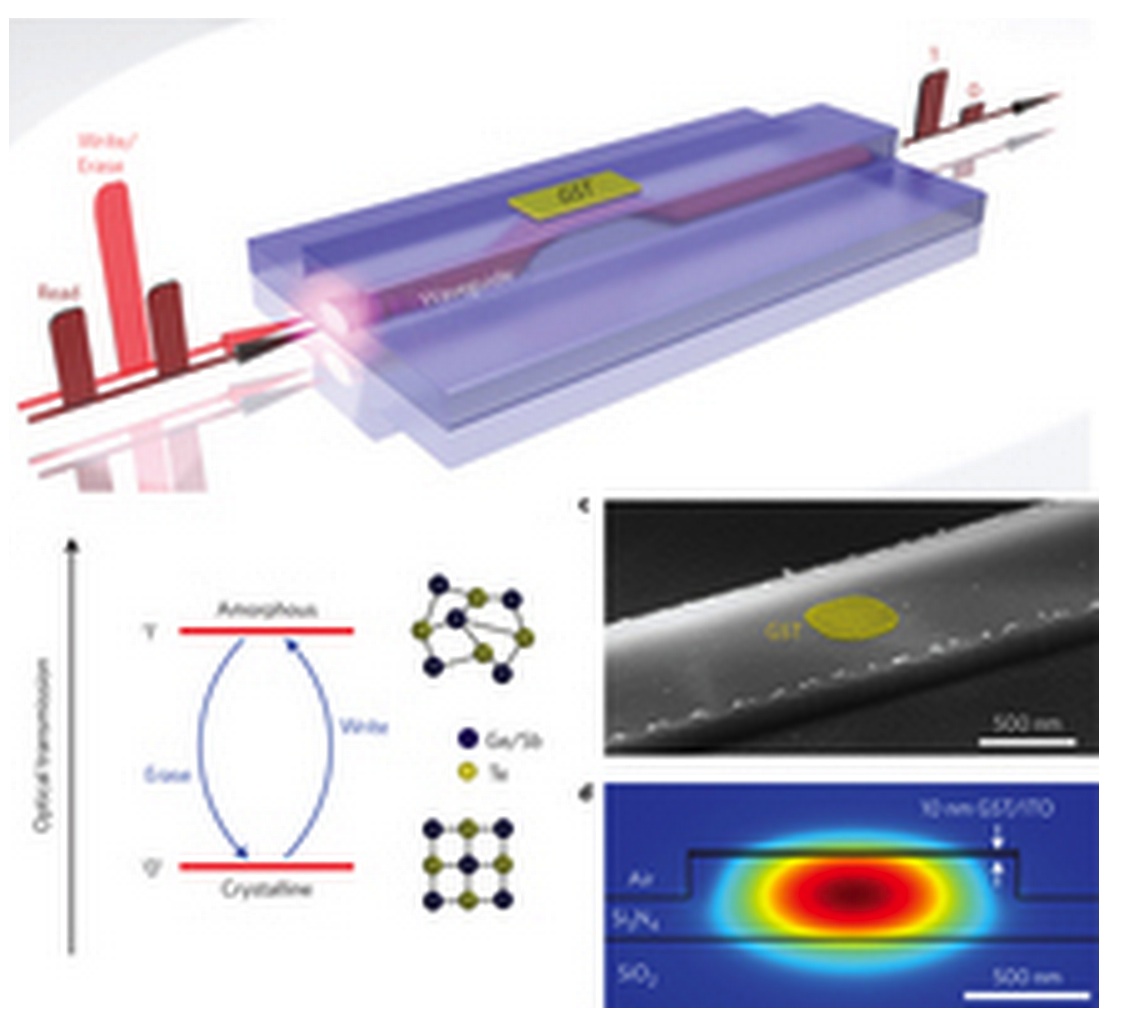
Information is stored in the phase state of the GST section on top of the nanophotonic waveguide.
Figure 2: Reversible and reproducible single-shot switching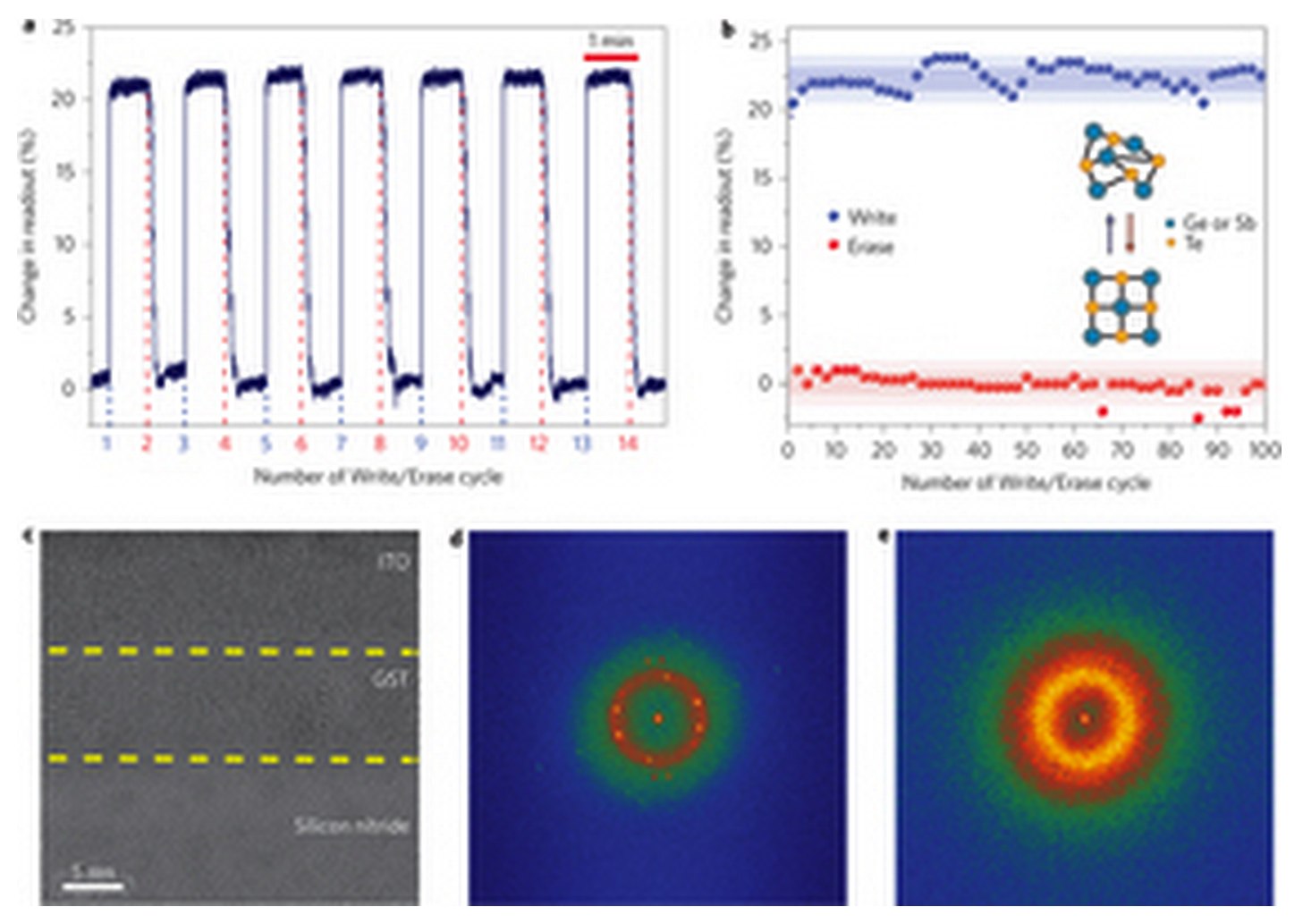
Demonstration of binary memory operation between the crystalline (lower, Level 0) and amorphous (upper, Level 1) state of a 5µm GST device with a total change in readout transmission of 21%.
Figure 3: A multi-bit, multi-wavelength architecture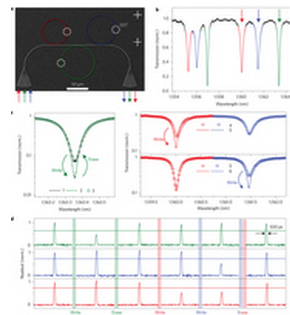
Scanning electron microscope micrograph of the device under test. Light is coupled in and out of the on-chip circuitry by means of the focusing grating couplers at the lower left and right.
Figure 4: Multi-level operation of the all-photonic memory element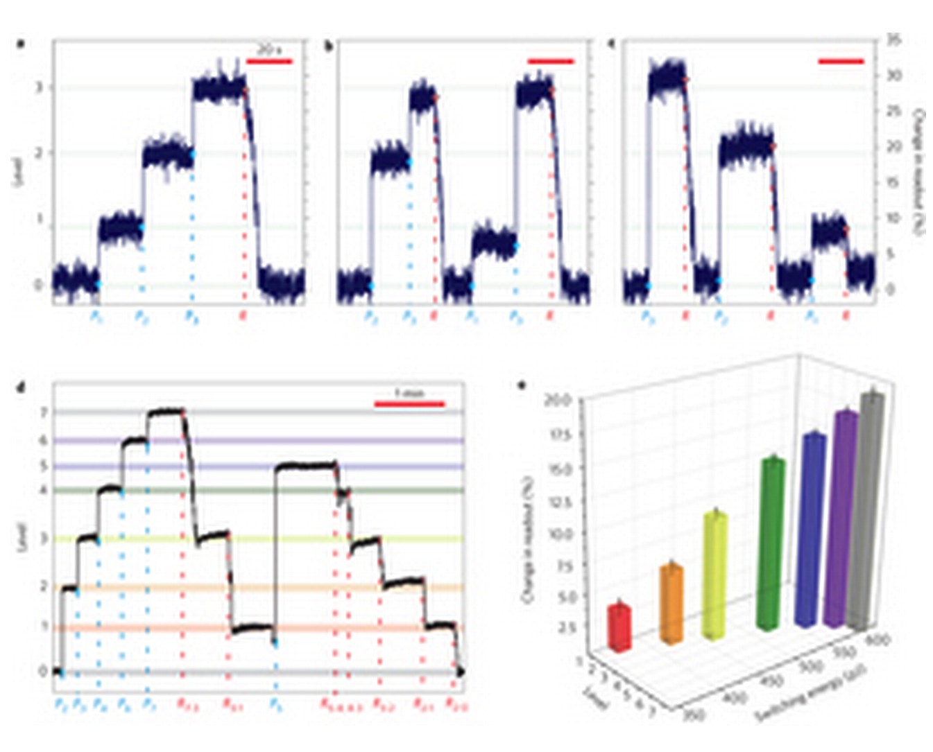
Four clearly distinguishable levels are reached with 100ns Write pulses Pi of level-specific energy EP1=465±13 pJ, EP2=524±14 pJ and EP3=585±14 pJ in a 5µm GST device.


 Subscribe to our free daily newsletter
