


NVMe IP for Enterprise SSDs
By IP-Maker
This is a Press Release edited by StorageNewsletter.com on March 29, 2016 at 2:58 pmThis white paper is published on the web site of IP-Maker, French company in NVMe compliant IP core, universal NAND flash controller and ECC.
NVMe IP for Enterprise SSDs
Abstract
The NVM Express (NVMe) specification has been introduced in 2011. Five years later, it is definitely adopted as the new standard storage interface for SSD. Even if SAS and SATA SSDs are still dominating the market (in unit shipment), the PCIe SSD market share is growing fast and will go over SAS and SATA.
Most of SSD manufacturers jumped into this new storage market with flash-based technology. A second wave of products will come in the near future, using a new generation of non-volatile memories, delivering impressive speed performances compared to NAND flash memories. The SSD manufacturers will have a to deal with low latency SSD controller design in order to benefit from the new NVM features, while keeping high reliability and low power consumption.
This white paper proposes a solution based on a full hardware NVMe implementation, describing its architecture, implementation and characterization.
The origin of NVMe
From HDD to SSD
The TCO of SSD-based system is becoming in the same range of systems running on HDDs, or even lower for configurations that require high performances. The price per gigabyte is higher, but it provides a higher ROI thanks to the performances. A HDD is limited to about 100 random IO/s due to the mechanics latency. A good SATA SSD can reach up to 70,000 IO/s. For an application that requires 10,000 IO/s, at least 100 HDDs will be used, but only one SATA SSD is enough, saving cost from drives, CPU, memory, software license and power consumption.
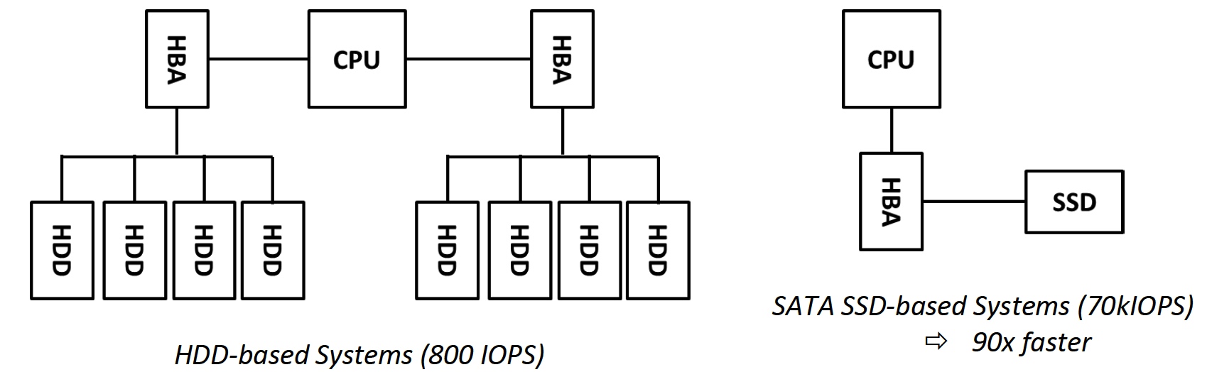
In the digital world where the demand of performance is increasing every day, we see the same comparison between SAS/SATA SSDs and PCIe SSDs. The second one is more expensive in term of dollars per gigabyte, but it provides about 10 times more performances in term of IO/s. Therefore, for application where the value is related to the performances, the choice of PCIe SSDs is the standard choice, providing the lowest TCO.
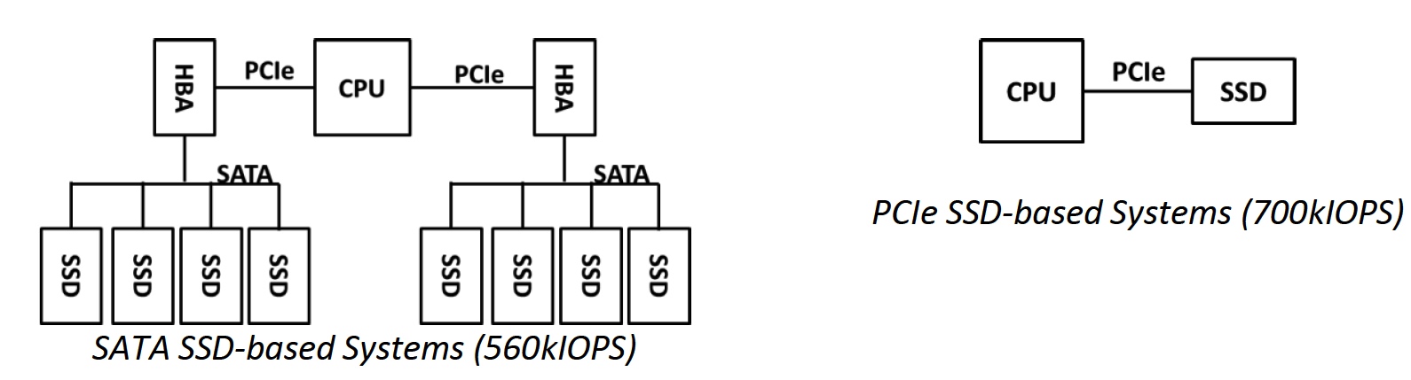
With faster non-volatile memories (NVM) and more powerful CPUs, the SATA/SAS interface is the IO/s bottleneck. The PCIe interface provides higher bandwidth and lower latency.
NVM and Multicore
NAND flash memory is the current used technology for SSDs. The memory read access is in the range of 50 microseconds and in the 1ms range for write access. Post-NAND flash memory will be available soon on the market. Intel and Micron announced the 3DXP technology in 2015, and many other players are working on equivalent technologies. This next generation of non-volatile memories (NG-NVM) such as 3DXP, RRAM or MRAM, come with higher performances than NAND flash, in the microsecond or below, for both read and write access.
In addition to the new generation of non-volatile memories, processing technologies are evolving with higher performances. Frequency speed is not growing any more, due to physics limitations, but architecture allows the integration of multiple cores. High-end CPUs come with up to 18 cores, while some ASSP comes with more than 200 hundred cores (manycore CPU). The CPUs are able to provide more computing capabilities, including IO management.
NVM express specification
As described above, current technologies allow the design of very fast SSDs based on fast memories, low latency PCIe interface, and high performance multicore CPUs on the host side. But what about the storage protocol? Using legacy protocols that have been designed for single core architecture and slow disks is not relevant. In addition, the first PCIe SSD manufacturers developed their own driver, adding development and qualification costs.
A new standard protocol was required: NVM Express.
NVMe was developed to reduce latency and provide faster performance with support for security and end-to-end data protection. Defined by 80+ NVM Express Work Groupwww.nvmexpress.org members, the specification, published in March, 2011, provides a flexible architecture for enterprise and client platforms. NVMe is an optimized, high performance, scalable host controller interface with a streamlined register interface and command set designed for Enterprise and Client systems that use PCIe SSDs. On the host side, the driver source code is available on the NVMe website, and is supported by the major OSs.
NVM Express benefits
- Driver standardization: an open source version is available from the NVM Express web site. Futur NVMe features, such as vendor specific commands, may integrate the standard driver
- Performance increase since the SATA bottleneck has been removed:
- Unlimited number of commands, NVM Express is able benefit from all the NandFlash resources in parallel (only 32 with SATA).
- Mutli queues management
- Faster serial bus with multi-lanes
- Reduced power consumption
Protocol
The NVMe specification defines a controller interface for PCIe SSD used for enterprise and client applications. It is based on a queue mechanism with advanced register interface, command set and feature set including error logging, status, system monitoring (SMART, health), and firmware management).
As a basic example, below is the protocol for a single write command.
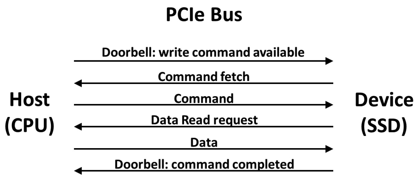
NVMe is a protocol encapsulated in PCIe data packet.
Here is the simplified write access description:
- 1- The host sets the configuration space of the device in order to inform it that there is a new submission queue ready
- 2- The device reads the submission queue into the host memory. The submission queue data includes the write access description (called submission command): source and destination address, data size, priority …
- 3- The device manages the data transfer
- 4- he device sends a completion queue to the host
Commands and queues
As explained above, NVMe is a submission/completion queue-based protocol. The commands are created by the host and placed in a submission queue. The completion queue is used to signal to the host the executed commands. It supports up to 64k I/O queues with up to 64k entries per queue. When a submission command is ready in the submission queue, the host indicates it to the device through a tail/head mechanism. Then the device fetches the submission command from the host memory. The submission command is executed according to its priority defined with an arbitration scheme. Each submission command is 64 bytes in size and is composed of a command identifier, an opcode, size, address and all information required for the submission command execution. The predefined submission commands are specific for data transfer which leads to a reduced list compared to the SCSI protocol.
The list includes administration and IO submission commands:
- Administration submission commands:
- Delete I/O Submission Queue, Create I/O Submission Queue, Get Log Page, Delete I/O Completion Queue, Create I/O Completion Queue, Identify, Abort, Set Features, Get Features, Asynchronous Event Request, Firmware Activate, Firmware Image Download, I/O Command Set specific, Format NVM, Security Send, and Security Receive
- I/O commands:
- Mandatory IO submission command: Flush, Write, Read
- Optional IO submission command: Write Uncorrectable, Compare, Write Zeroes, Dataset Management, Reservation Register, Reservation Report, Reservation Acquire, Reservation Release
Enterprise Grade: performance and reliability
Latency
There are multiple definitions for latency. Therefore this paper will not provide a detailed definition, but some parameters to take into account when discussing latency numbers.
Start and stop time: The latency defines the time between a request and its completion. In case of a SSD, one might ask, what is the start time? Or when does the data transfer on the host side initiate?, or when does the SSD receive the request? The difference is simply a subsystem latency or a system latency.
What about the stop time: Is it the end of the full data transfer? Or is it when the first data is on the bus?
Another parameter is the data size when considering the latency as the full time including data transfer. For PCIe SSD, latencies are provided for an IO size of 4KB, 512B or less. The transfer time will not be the same, leading to differences in the latency numbers.
In addition, the provided latency in the documentation of a SSD is the latency measured when using it for the first time. In this case, the memory is empty and access is quite fast: less than 100 microseconds, or even lower when cache mechanisms are used; but after a few hours of running, the latency range is more in the millisecond range, or at least few hundred of microseconds.
So, when talking about latency, be sure to have the same definition.
Queue depth
The queue depth (QD) is related to the number of commands executed in the same batch. A queue depth of 1 means that the host will wait for the completion of this single command before sending a new command. A queue depth of 8 means that 8 commands will be processed in the same batch. The IO/s performance is related to the queue depth and the latency. In order to reach the maximum number of IO/s, SSD manufacturers typically use benchmark with QD=256. In the real life of applications, the queue depth is between 8 and 32.
IO/s
It’s important to understand IO/s numbers. Storage manufacturers typically communicate with best case IO/s numbers. But for which PCIe configuration? Which IO size? Which Queue Depth? Here is a description of the theoretical maximum number of IO/s on a PCIe Gen2 x4 configuration.
The IO/s is one of the key performance parameter for a storage system. The other parameters are the latency (in microseconds or milliseconds), and the throughput (MB/s). The size of the IO is generally 4kB, and the results are provided in kIO/s. The typical measures listed in storage documentation are done for read and write, random and sequential accesses. In benchmarks studies, additional measures are done like R/W (70/30).
A Gen2 lane speed is 5Gb/s. With 4 lanes, the overall speed is 20Gb/s. It would be too easy to do the following calculation: 20Gb/s divided by 4,096B, equal to 610K IO/s! The real value must take into account at least 3 parameters: the 8/10 bit coding, the PCIe overhead, and the fact that a bus can’t be used 100% of the time. The first factor, the 8/10bit coding, basically results in 80% of real information transferred on the PCIe bus. The second factor is the PCIe overhead. In addition to a data packet, multiple added bytes are included in the data transfer, such as sequence number, header and CRC. That leads in a 20 or 24 bytes overhead. Let’s do the calculation with the typical payload (data packet size) of 256B. 280B are used to transfer 256B, resulting in a 256/280=91% efficiency. Finally, the PCIe bus occupancy rate is estimated as 90%.
Therefore, the maximum IO/s is 610K x 80% (8/10b coding) x 91% (PCIe overhead) x 90% (PCIe bus occupancy rate) = 400k IO/s. This is the maximum that we can reach, assuming data transfer without any protocol or any command management. Unfortunately, it is impossible to send/receive data only on the bus of a PCIe SSD. A protocol is required in order to provide mandatory information in addition to the data (address, packet size, priority, system information, …). The NVMe specification defines an optimized register interface, command set and feature for PCIe SSDs. The necessary commands for the data transfer will add traffic on the PCIe bus, resulting in a performance loss compared the theoretical maximum 400K IO/s. This loss is estimated as 5%, leading to 400K IO/s x 95% = 380K IO/s. This is the maximum IO/s performance to be observed on an optimized storage system using a NVMe PCIe Gen 2 x4 interface.
Performance for intensive applications
Why do we need systems with low latency? Social networks are good examples, such as a server receiving millions of requests that need to be able to access the storage media with the lowest time; this is not the only case that also includes data base requests, big data analytics, in-memory computing, etc. For all these businesses, a higher latency means a lower transaction number each day, which is often closely linked to revenue. In a few words: time is money.
It is easy to understand that low latency will provide benefits to the above applications, but there are other ways to benefit from low latency NVMe drives. In a software-defined infrastructure, the resources are virtualized. This flexible server management is feasible with fast connections between storage and compute, even on different racks. For that, the NVMe specification is being adapted to other physical layer (Ethernet, IB, FC, …) in order to keep advantages of low latency from NVMe, this is called NVMe over Fabrics.
Reliability
Reliability, one of the most important criteria for an enterprise storage system. Losing data is not allowed. How is a storage system reliable? The main potential issues are the memory corruption, a controller failure and performances coherency which may lead in an availability issue. The expected reliability from the IT manager is defined with a 99.999% availability. Below is a short list of features to integrate in a NVMe SSD in order to reach the five nines.
QoS: This is often related to the latency. SSD manufacturers communicate often with the lowest latency number (e.g 20 microseconds) but IT manager will look at the 99.99%%ile latency (e.g. few hundred of microseconds). Therefore, the internal SSD management, including NVMe protocol processing, must be designed in order to ensure a low latency in any cases.
Redundancy: All flash arrays are typically based on a dual controller architecture. There is an active and a standby controller. That allows the access to the SSDs even if a controller has failed. On the SSD side, that means that each SSD is accessible by the two controllers. A switch mechanism is required at the front of the SSD, or as a better solution, a dual port interface can be integrated inside of the SSD. That can be done by using two PCIe interfaces.
Data protection: The data coming from the host are going through many interfaces and memory buffer: PCIe interface, internal RAM, CPU, external DRAM, flash memory, … Then at each step, there is an opportunity to get corrupted data due to power spikes for example. In order to ensure end to end protection, some specific mechanism must be integrated. It is well defined by the T10 organization.
ECC: NAND flash memory is well known to have limited endurance (few hundreds to few thousands cycles). When reaching this limitation, bits may be corrupted in the memory. Then, an ECC is required in order to detect and correct the corrupted data. This is included in the SSD controller, in software or hardware. Common ECC are based on a BCH technology. LDPC are better for coming NAND flash memories. LDPC allows to correct a higher number of errors.
What about NVMe and Reliability?
The NVM express specification has been defined for both enterprise and client SSDs. Therefore, reliability features can be easily integrated.
NVMe SSD Design
Architecture
IP-Maker has developed its own NVMe IP, from the ground-up, to be integrated in SSD controllers. Using pre-validated NVMe IP core, allows to greatly reduce time-to-market for storages OEM which want to benefit from a powerful NVMe compliant solution. The IP-Maker NVMe IP core is full featured, easy to use into both FPGA and ASIC designs.
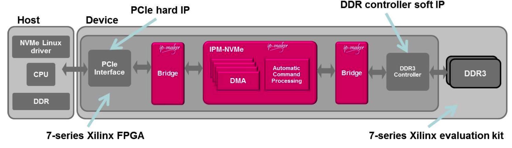
Below is the architecture of the NVMe IP from IP-Maker. All the different part required by the NVMe specification have been designed through multiple hardware blocks, including configuration space, queue context management, queue arbitration and R/W DMA engines.
NVMe SSD controller based on IP-Maker NVMe IP technology 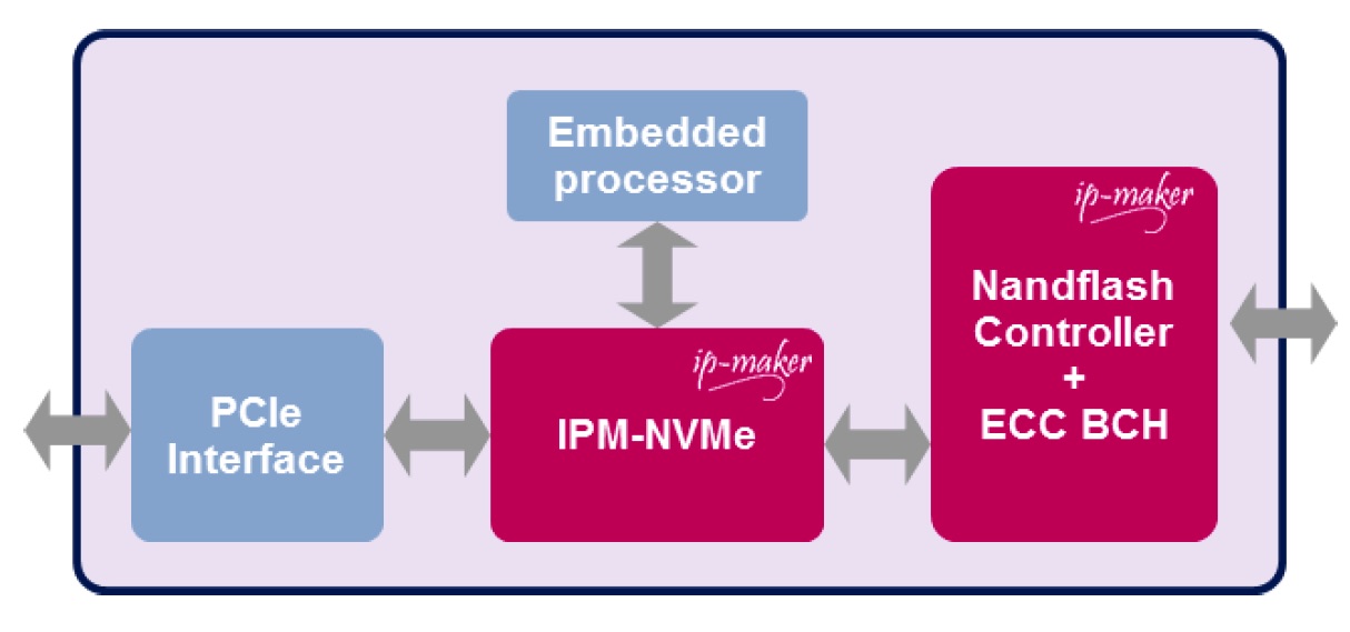
Each of the hardware blocks takes only few clock cycles to be processed, therefore reducing dramatically the NVMe processing latency. So the impact of the NVMe processing on the system latency is very low compared to the other latency parameters.
The NVMe commands are processed by an automatic command processing unit. The data transfer rate is accelerated with the multi channels DMA integrated in the read and write engines (read and write DMA channels are independent and can operate in parallel). So, the PCIe bus is always used by NVMe accesses. The maximum throughput is defined by the PCIe configuration: number of lanes and speed generation.
This full hardware NVMe architecture is ideal for persistent memories, such as 3DXP, NVRAM, MRAM or RRAM.
Command processing unit
IP-Maker has implemented a full hardware architecture for the NVMe commands. That includes the different steps: fetching, arbitration and execution. This Automatic Command Processing Unit is connected to a multi-channel DMA to perform data transfers
All the fetching is automatically done in hardware with dedicated customizable DMAs. The different arbitration rules such as round robin have been designed in a dedicated hardware block. The commands are executed by a NVMe command engine. The additional features are also managed in hardware, including the queue context management, the interrupt management, the asynchronous event and error log page.
All administration submission commands and mandatory NVM IO submission commands are processed in hardware, without use of an external processor. In case of a read or write command, the DMAs are triggered to perform the data transfers, leading to a full hardware implementation of the NVMe specification. A CPU may be required to provide flexibility like for vendor specific commands. This architecture is easy to integrate with standard interfaces, between the PCIe and memory controllers.
Multichannel DMA
The multi-channel DMA is configurable, up to 32 channels for read and up to 32 channels for write. The DMA engines are activated as soon as a memory transfer command is fetched by the automatic command processing unit. Using multiple channels allow to perform data transfer all the time, avoiding transfer stop when the data are read or written in the memory. NVMe is based on a queue mechanism. Multiple commands can be used in one queue. For latency optimization, the best is to use one command per queue. But for data transfer, it is recommended to increase the number of commands in a single queue (e.g. 1,024 commands per queue).
Reliability
The way to manage and process the NVMe protocol may have an important impact on the QoS. When based on a full software implementation, the processing time may change according to IRQ management. If based on a full hardware architecture, the processing time is deterministic and will provide a good system latency QoS.
Using a full hardware NVMe implementation is more easy to use with a dual PCIe interface. A NVMe IP can be used on the back end of each PCIe controller, or only one can be used, shared by the PCIe controllers. The second case seems to be easier to manage. The use of a tag system will help in identifying which PCIe controller is accessing the NVMe IP.
Test and verification
Reference design
The NVMe IP has been integrated in a FPGA-based reference design. It is based on Xilinx FPGA. The NVMe IP is connected to the PCIe hard IP and a soft DDR3 controller IP. It is configured as Gen2 x4. The storage part of this NVMe reference design is based on a 2GB DDR3 memory in order to demonstrate the NVMe IP performances.
 On the host side, a server platform is running Linux Fedora 17 with the NVMe driver. When installed in the PCIe slot, the NVMe reference design is detected as a NVMe storage device. The performances are measured with the standard FIO tool (GFIO version with GUI).
The latency numbers have been measured with GFIO, a standard tool for storage benchmarking:
GFIO user interface
Click to enlarge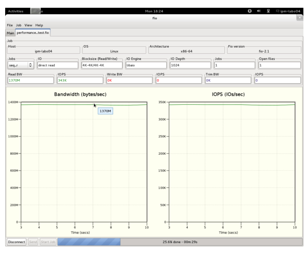
The results of GFIO show a 380K IO/s (the maximum on a Gen2 x4 configuration), in both sequential and random 4KB IOs. On the latency side, it leads to 12 microseconds (QD=1, IO= 4KB). This latency budget is split between 3 microseconds for data transfer setup, and 9 microseconds for data transfer completion. A data transfer setup includes: a file system setup and an NVMe driver setup. Completion time includes: doorbell register write access, submission command fetching, data transfer, and completion command. The latency budget coming from the IP-Maker NVMe IP is only few hundred of nanosecondss.
Other tools, such as a protocol analyzer may be used in order to screen all the NVMe transaction details.
Compliance test
In order to be NVMe compliant, a SSD product must pass the official test suite managed by the University of New Hampshire Interoperability Lab (UNH-IOL). The conformance tests are based on the UNH-IOL NVM Express Conformance Test Suite Document release by the NVM Express work group. UNH-IOL provides NVM Express conformance testing.
The reference design from IP-Maker has successfully passed the NVMe compliant test in 2015. The company is part of the official NVMe integrator list.
Conclusion
This NVMe hardware implementation combines the benefits of an ultra-low latency, a reduced power consumption and a limited silicon cost. Therefore it is an ideal solution for high performance storage systems. Industry leaders will benefit from the enterprise grade without adding cost. In addition, it is ready to support next generation of NVM, which comes with better performances in term latency, density and power consumption.


 Subscribe to our free daily newsletter
